[Most Recent Entries] [Calendar View]
Tuesday, January 8th, 2013
| Time | Event | ||||||||||||||||||||||||||||||||||||||||||||||||||||||||||||||||||||||||||||||||||||||||||||||||||||||||||||||||||||||||||||||||||||||||||||||||||||||||||||||||||||||||||||||||||||||||||||||||||||||||||||||||||||||||||||||||||||||||
| 1:53a | Qualcomm's Next-Gen Krait 400 & Krait 300 Announced in Snapdragon 800 & 600 SoCs
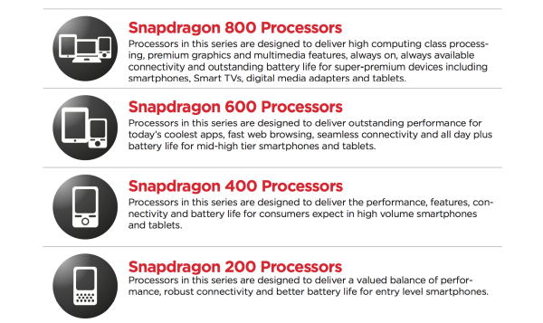
We've been hinting at this for a while, both on the Podcast and in our most recent power analysis piece, but today it's very official: Qualcomm is announcing the next two versions of its Krait architecture. Krait is the codename for Qualcomm's custom ARMv7 microprocessor. The 3-wide out-of-order design dominated the smartphone landscape since its introduction last year. Unlike what we saw with the Scorpion/Krait transition, Qualcomm is going to keep Krait fresh by more frequent updates. The first two updates come today: Krait 300 and Krait 400. Krait 300 In usual Qualcomm fashion, we're missing good depth on exactly what these new revisions deliver. This is one area where Qualcomm really needs to emulate Intel: we know more about Haswell than we do about the original Krait. That being said, here's what we do know. Krait 300 is still built on TSMC's 28nm LP process, just like the original Krait. The pipeline remains unchanged, but Qualcomm is able to squeeze out higher clocks out of the core. It's unclear whether we're simply talking about voltage scaling or a combination of that and improvements to timing, yields and layout. Whereas the current Krait core tops out at around 1.5GHz, Krait 300 will run at up to 1.9GHz. Another big addition to the architecture is Krait 300 now features a hardware data prefetcher that preemptively grabs data out of main memory and brings it into L2 cache. The original Krait core had no L2 prefetchers. Single threaded IPC improvements are the name of the game with Krait 300 and like all good evolutions to microprocessor architectures, the new Krait improves branch prediction accuracy. Since there's no increase to pipeline depth, improved branch prediction directly results in improved IPC (and better power efficiency). Both Qualcomm and ARM have been very vague about what types of instructions can be executed out of order, but Krait 300 can execute more instructions out of their original program order. Building a robust OoOE (Out of Order Execution Engine) is very important to driving higher performance, and being able to reorder more types of instructions directly impacts single threaded performance. Krait 300 now supports forwarding between pipelines, although it's not clear whether or not the previous architecture lacked any ability to forward data between stages. Finally Krait 300 improves FP and JavaScript performance. Once again, it's not clear how. I've asked Qualcomm whether there have been any changes to the execution units in Krait 300 to enable these improvements. In general I believe we're looking at around a 15 percent increase in performance at the same clock frequency, for a jump of 20 to 30 pecent overall with the clock increases. This isn't necessarily enough to close the gap between Krait 300 and ARM's Cortex A15, however Krait 300's power profile should be much better. Compared to Atom, the Krait 300 improvements should be enough to at least equal performance if not surpass it, but not necessarily significantly. Krait 400 If Krait 300 is the new performance mainstream successor to Krait, Krait 400 is the new ultra high end part. Using TSMC's new 28nm HPm process (High-K + Metal Gate, optimized for low power at peak performance), Krait 400 can run at up to 2.3GHz. The 400 series core inherits all of the improvements from Krait 300 but adds a couple more. The move to 28nm HPm necessitates a redesign of circuits and some relayout, but Qualcomm also improved the memory interface on the core. Krait 400 enjoys lower latency to main memory and a faster L2 cache. The New Snapdragons The new Kraits will find their way in new Snapdragon platforms, now numbered 200, 400, 600 and 800 (the old S1 - S4 labels are gone). As always, higher numbers mean better performance but you'll still need to rely on the internal part numbers to know what's really inside. Today Qualcomm announced the Snapdragon 800, which implements four Krait 400 cores running at up to 2.3GHz, an Adreno 330 GPU and Qualcomm's 3rd generation LTE baseband (9x25) all on a single die. Snapdragon 800 is the part formerly (or still internally) known as MSM8974 which we've seen rumblings about numerous times. Qualcomm tells us that the Adreno 330 will offer roughly 50% more graphics performance over Adreno 220, and an almost 2x increase in compute performance. The integrated 9x25 3rd generation LTE baseband enables support for UE Category 4 LTE with up to 150Mbps downstream, this is the same IP block as in MDM9x25, and likewise MSM8974/Snapdragon 800 will be available in all the usual variants (CDMA2000/WCDMA/LTE, WCDMA/LTE, and finally no modem). Snapdragon 800 also integrates 802.11ac baseband, a new feature of modern Qualcomm SoCs, just like 8960 and the previous S4 family. Snapdragon 800 also includes a 2x32 LPDDR3 memory interface. On the video/decode side, the SoC supports encode/decode of 4K HD content at 30 fps. Also being announced today is the Snapdragon 600. This part integrates two Krait 300 cores running at up to 1.9GHz. Adreno 320 handles GPU duties, although with an increased clock speed. Compared to the current Snapdragon S4, the 600 is expected to improve performance by up to 40% if you combine IPC and frequency increases. The new Snapdragon 600 is also known by the part number APQ8064T, and was formerly known as the Snapdragon S4 Pro. Final Words Qualcomm really is the one to beat when it comes to smartphone SoCs. Its excellent baseband integration combined with a very good balance of power and performance on the CPU/GPU side make for a platform that's difficult to outperform. With Krait 300/400, Qualcomm is really evolving its Krait architecture the right way. The update comes at the right time after the original Krait, and improves performance in the right way. A religious focus on improving single threaded performance, generation over generation, without blowing through your power budget is the only way to do this. Qualcomm gets it. Krait was good, but Krait 300/400 are likely going to continue to carry that flag through 2013. More importantly, Qualcomm has hinted numerous times that it has a "pipeline of Kraits" lined up for the future. In tablets and larger devices are really where Qualcomm will have its work cut out for it. Between Intel's x86 offerings and ARM's Cortex A15, Qualcomm's strengths still apply - but they're going to face more strenuous competition. Today's announcements are a welcome update. Qualcomm is gearing up for a war and is definitely making the right moves. If it can keep up this aggressive cadence, Krait can easily become a fixture in the ultra mobile space.
| ||||||||||||||||||||||||||||||||||||||||||||||||||||||||||||||||||||||||||||||||||||||||||||||||||||||||||||||||||||||||||||||||||||||||||||||||||||||||||||||||||||||||||||||||||||||||||||||||||||||||||||||||||||||||||||||||||||||||
| 3:20a | AMD’s Annual GPU Rebadge: Radeon HD 8000 Series for OEMs
In an effort to mimic the model year nature of cars and other durable goods, in recent years PC OEMs have increasingly moved to updating their wares both on a technical basis and on a calendar basis. Of course with the technical cycles being 15-18 months as opposed to a 12 month calendar cycle, this means that OEMs are often put into a position where they’re doing their yearly refresh in the middle of a technical cycle, and 2013 is no different. This of course gives rise to the annual rebadge cycle that we have become familiar with over the years. We’ll see a number of “new” desktops and laptops at CES this year. But along with rebadging the systems themselves, the pressure to rebadge has been pushed down to the component suppliers, which means that powering these “new” systems we’ll see a number of “new” components. In the GPU world both AMD and NVIDIA make an annual event of this, which for market reasons are roughly timed to coincide with CES. Kicking the GPU rebadge cycle off this year is AMD, who along with their press conference today also pushed out their rebadges. Let’s jump right into the thick of things. Desktop Because the rebadge cycle is OEM driven, rebadging is typically focused exclusively on OEM parts, and this year is no exception. The Radeon HD 7000 series isn’t going anywhere in the retail market, but in the OEM market where OEMs are demanding parts with higher numbers, the entire Radeon family from top to bottom is getting rebadged. This means everything from the powerhouse Radeon HD 7970 GHz Edition to the diminutive (and ancient) Radeon HD 5450 are getting 8000 series product designations. AMD to their credit has kept their retail desktop lineup consistent in naming and features, but with the OEM lineup this has gone completely out the window.
The OEM 8900 series are rebadges of the 7970GE and 7950 w/Boost respectively. Meanwhile the sole 8800 part, the 8870, is a rebadge of the 7870. Further down the list the 7700 series is composed of a rebadged 7770 and 7750-900 (which never saw a proper launch outside of China). Farther down the lineup still, we actually see a break from rebadging with the introduction of new desktop parts. AMD’s recently announced Oland GPU, which are the very last members of the first generation of the GCN family (and not members of AMD’s forthcoming refresh), will be joining AMD’s OEM desktop lineup as the 8670 and 8570. With only 384 SPs these budget GPUs are not particularly potent, and we wouldn’t at all be shocked if these GPUs never come to the retail desktop market. The real question right now is where they stack up against iGPU solutions such as Trinity’s HD7600 GPUs or Intel’s HD4000, or NVIDIA’s equally low-end desktop GK107 cards like GT 640 and GTX 650. Finally at the bottom of AMD’s OEM 8000 series stack are some of the oldest AMD GPUs still in production, and decidedly not GCN parts. The 8400 series is a rebadge of various configurations of the Radeon HD 6450 (Caicos GPU, VLIW5). Meanwhile the 8300 series is a rebadge of the ancient VLIW5 Cedar GPU, first introduced in 2010 as the Radeon HD 5450. Frankly it’s not at all clear at this point in time just what the purpose of these final rebadges are, as these cards are slower than a good iGPU. APAC markets are even more heavily weighted towards budget components than the North American market already is, so it’s quite likely that these cards are meant to fill APAC-specific product needs.
| ||||||||||||||||||||||||||||||||||||||||||||||||||||||||||||||||||||||||||||||||||||||||||||||||||||||||||||||||||||||||||||||||||||||||||||||||||||||||||||||||||||||||||||||||||||||||||||||||||||||||||||||||||||||||||||||||||||||||
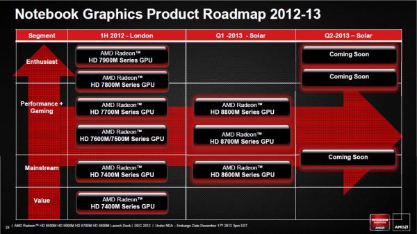
| 4:15a | AMD Releases Full Product Specifications For Radeon HD 8000M Series Along with their announcement of their annual desktop GPU rebadge, AMD has also released the full product specifications for their new Radeon HD 8000M mobile GPUs. These GPUs were first announced back in December, but at the time AMD only gave us vague descriptions of each series with little-to-no information on the individual SKUs. Now with CES kicking into gear, we have the individual SKU information on hand.
Starting at the top is the 8800M series, which is composed of a number of not-quite rebadges of 7800M parts. All of these GPUs are based on the Heathrow GPU (desktop name: Cape Verde), packing 640 Stream Processors along with 40 texture units and 16 ROPs. This is paired with 2GB of memory on a 128bit bus, with AMD using both GDDR5 and DDR3 depending on the specific SKU. Other than being minor variations on existing AMD GPUs, these products also enable AMD’s Boost Clock technology for the first time in a mobile part. Boost Clock allows the GPU to turbo up to a higher clockspeed so long as the GPU is under its power and temperature limits, allowing AMD to scrape every bit of thermal headroom from their GPUs. This technology has been available on certain desktop GPUs for more than half a year, but this is the first time we’ve seen it on a mobile part. Notably, NVIDIA’s mobile parts do not feature NVIDIA’s equivalent technology (GPU Boost) despite the fact that they introduced the technology on the desktop first, so AMD is ahead of NVIDIA in this regard.
Below the 8800M series is the 8700M series, marking the introduction of AMD’s new Mars GPU. This is a 4th (and presumably final) first-generation GCN GPU, packing 384 stream processors, 24 texture units, and 8 ROPs. The 8700M is connected via a 128bit memory bus to 2GB of either GDDR5 or DDR3 depending on the SKU, and like the 8800M series also features AMD’s Boost Clock. Interestingly, all Mars products only offer a PCIe 8x bus instead of the GPU industry standard 16x. The performance difference on these lower-performance parts should be miniscule, but it’s an example of one of the ways AMD was able to achieve their smaller die size by reducing the number of pins that needed to connect to the GPU.
Finally we have the 8600M and 8500M series. These are essentially cut-down Mars parts, halving the memory busses from 128bits wide to 64bits wide, and should significantly castrate performance in the process. The feature set and functional unit counts are otherwise identical to the 8700M series. The difference between the 8600M and 8500M series appears to come down to solely clockspeeds; the 8600M parts are clocked up to 775MHz, while the 8500M are clocked up to 620MHz/650MHz.
| ||||||||||||||||||||||||||||||||||||||||||||||||||||||||||||||||||||||||||||||||||||||||||||||||||||||||||||||||||||||||||||||||||||||||||||||||||||||||||||||||||||||||||||||||||||||||||||||||||||||||||||||||||||||||||||||||||||||||
| 8:07a | Hands On with the Huawei Ascend W1, Ascend D2, and Ascend Mate
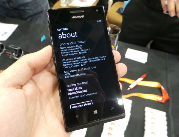
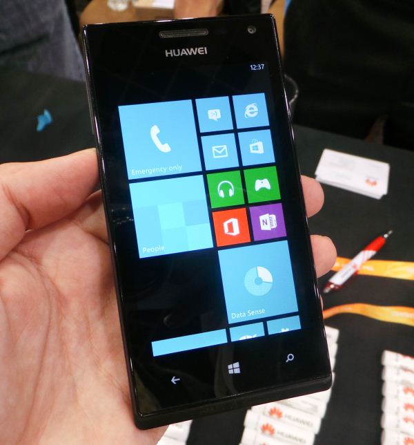
There hasn't been much in the way of mobile handset news out of CES 2013 this year, save some announcements by Huawei this morning. I didn't get a chance to make it into the Huawei press event, but instead caught up with Huawei at Pepcom this evening and got my hands on the three devices that were announced. Huawei Ascend W1 Probably the most intriguing handset from Huawei is their first Windows Phone 8 device, the Ascend W1 (H883G). Huawei is entering the market with a decidedly entry-level set of specs with the W1, but it's an impressive first beginning. The W1 is based around a 1.2 GHz Snapdragon S4 Plus (MSM8230) SoC and 512 MB of LPDDR2, and looking at the menu, resolution on the 4-inch IPS display is WVGA. There's a 0.3 MP front facing camera and 5 MP rear facing camera as well. The W1 comes with 4 GB of internal storage, but behind the removable battery cover is a microSD card slot. Those specifications align pretty closely with other midrange or entry level WP8 devices, like the HTC 8S, and there's a definite place for them in the grand scheme of things.
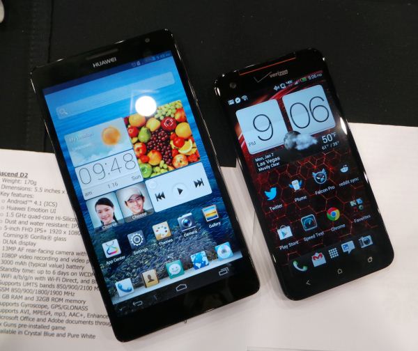
Gallery: Huawei Ascend W1       The hardware is a bit thicker than I'd like for a WP8 device, but the tradeoff gets you removable battery, microSD, and (given it's Huawei) probably one of the most affordable price points around. There's no word on what that eventual pricing will be or whether any operators have already expressed interest but I'd say Huawei making inroads with its entry level WP8 device is inevitable. Huawei Ascend MateNext up are Huawei's two new Android phones, both based around (Huawei) Hisilicon's own K3V2 SoC. I've been trying to get an Ascend D1 in so we can take a closer look at Huawei's K3V2, which consists of 4 ARM Cortex A9 CPUs clocked at up to 1.5 GHz for one core, 1.2 GHz for all four, 16 core Vivante GPU, 2x32 LPDDR2 memory interface, and all built on 40nm process. I've been interested in the K3V2 for some time, as Huawei joins one of a small number of handset makers serious enough about being vertically integrated to make its own SoC and (in the case of the D2) also baseband. Anyhow the real key pointer with the Ascend Mate is its gargantuan 6.1-inch IPS display which cirously enough is only 720p. The Mate is a seriously beefy phone, and although it fit in my hand I think manipulation does require two hands in this case.
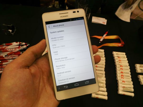
Gallery: Huawei Ascend Mate       The Mate has an 8 MP rear facing camera, 1 MP front facing camera, 802.11a/b/g/n, BT 4.0+LE, and runs Android 4.1. Just like a bunch of prior Huawei phones, the Mate also is pentaband WCDMA (850/900/1900/2100/AWS) courtesty Intel's incredibly ubiquitous XMM6260 baseband and RF combo. Battery is a respectable 4050 mAh (I'm guessing at 3.7V, so just shy of 15 watt-hours). Huawei Ascend D2 The phone from Huawei Device I'm probably most interested in is actually the Ascend D2, which a much more modestly sized device with a 5-inch display, running Android 4.1. The D2 departs from the Mate by packing a much nicer speclist on paper. That 5-inch display is 1080p, rear facing camera is 13 MP, front facing is 1.3 MP, there's 2 GB of LPDDR2, 32 GB of internal storage, and the device is IPX5/4 dust and water resistent respectively. What's most interesting to me however is that this is Huawei Device's first smartphone with both their own SoC (again the K3V2 A9MP4 + Vivante GPU), but more interestingly a Balong V7R1 baseband for cellular connectivity. I've heard of the Balong 710 which is Huawei's LTE Category 4 baseband, but am not sure whether V7R1 refers to this part or something else which only tops out at WCDMA. Huawei clearly feels strongly about its modem, touting their DRX (Discontinous Recieve) and QPC (Quick Power Control) features quite vocally. Either way this is a very big interesting step for Hisilicon and Huawei to take and I very much want to play around with the Ascend D2 at some point.
Gallery: Huawei Ascend D2       Industrial design on the D2 clearly borrows from some other devices, but construction felt very impressive and solid. It has been clear for some time that Huawei can craft devices of their own at very competitive price points without sacrificing design.
| ||||||||||||||||||||||||||||||||||||||||||||||||||||||||||||||||||||||||||||||||||||||||||||||||||||||||||||||||||||||||||||||||||||||||||||||||||||||||||||||||||||||||||||||||||||||||||||||||||||||||||||||||||||||||||||||||||||||||
| 12:00p | Broadcom Unveils 4Kp60-capable BCM7445 SoC for Home Gateways (STBs) The unveiling of the BCM7445 is undoubtedly the most exciting news to come out of the Broadcom camp for CES 2013. It is the fourth generation STB (set-top-box) SoC from Broadcom and the industry's first 28nm product for the market. Before going into the details of the BCM7445, we present a couple of subsections to provide a little bit of background about 4K video and related technology. If you are interested in learning about Broadcom's 4Kp60 capable BCM7445 alone, feel free to skip right ahead. The Need for 4K One of the main challenges being faced by the TV industry after the failed 3D experiment is a way to stimulate the consumer base. In this context, the 4K experience is proving to be quite effective. Journalists may argue about whether 4K makes sense for the living room or not, but the truth is that increasing the resolution of the content reaching the consumers is the first step towards an immersive entertainment solution in the future. Unlike 3D, 4K has legitimate industry uses in the medical imaging and IP surveillance industry. This gives an impetus for silicon vendors to create 4K-capable products without worrying about whether the consumer industry might accept it or not. In addition, given that there is nothing to dislike about 4K at this point other than the price tag, it looks like 4K will gain much better acceptance compared to 3D technology amongst the consumers. 4K: Should You Be an Early Adopter? Last year, we reviewed the AMD 7750 and GT 640 from a HTPC perspective and were able to get both cards to drive a 4K projector (the Sony VPL VW1000ES) using the following 4K resolutions: 3840x2160 at 30 Hz and 4096x2160 at 24 Hz. Simply speaking, higher refresh rates are not possible because the frequency of operation of the HDMI controller / PHY doesn't provide enough bandwidth. A refresh rate of 50 / 60 Hz is required to provide smooth movement in scenes with fast transitions. HDMI 2.0 (the name going around the industry, despite the HDMI forum's decision to do away with version numbers for all HDMI products) is going to be ratified soon, and will apparently simply double the operating frequency of the controller / PHY to provide enough bandwidth to send across uncompressed 4Kp60 video. The high cost of current 4K solutions is already a deterrent, and if one is hesitating to jump in right now, these facts should serve as an incentive to wait for some more time. Contrary to popular belief, there is really no dearth of 4K content since most professional videographing solutions have been 4K capable for a number of years. It is a simple matter of bringing that content in the right format to the end-consumer. H.264 emerged as the codec of choice (and replaced MPEG-2 due to better compression efficiency) when moving from SD to HD. However, both H.264 and MPEG-2 co-exist in the Blu-ray standard for HD content. Similarly, H.265 (HEVC) is expected to become the codec of choice (and replace H.264 due to better compression efficiency) when moving from HD to 4K. However, consumers can expect a lot of the initial 4K end-user content to be in H.264 format (such as the current 4K videos on YouTube or the 4K videos being shot on the GoPro Hero 3 Black). All said, a future-proof 4K solution should have the capability to decode 4K content in both H.264 and H.265 (HEVC) formats. Broadcom's BCM7445 The BCM7445 is a STB solution aimed at making its way into service provide boxes (such as those from Comcast or Dish). In addition to implementing all the necessary security measures for a conditional access system, the SoC also integrates a programmable multi-format decoder (including H.265 / HEVC) and the ability to transcode up to four 1080p30 streams in real-time. The master processor in the SoC is the Brahma15, a quad-core Cortex A15 configuration running at up to 1.5 GHz to provide 21000 DMIP performance. The configuration has TrustZone, NEON and virtualization support. Plenty of performance is needed to run Broadcom's Nexus and Trellis multi-framework software interfaces which allow different client technologies to operate in a seamless manner. Broadcom refused to divulge power consumption details (a very important aspect since set top boxes happen to be one of the worst offenders when it comes to home energy consumption), but did indicate that their platform supports on-chip power management to power down unused blocks in the chip as applicable. We asked Broadcom whether the appearance of the Cortex A15 in a STB SoC marked the beginning of the end for MIPS in the STB space. They were quick to point out that they continue to be solidly behind MIPS for multiple segments of the STB market and indicated that it was one of their MIPS-based STB platforms (BCM7356 in the Samsung SMT E-5015) that had obtained official Android 4.0 certification recently. Samples of the BCM7445 are available now with volume production scheduled for mid-2014. This should give the 4K market plenty of time to mature. We will visit the Broadcom booth at CES and see the 4Kp60 demo in person. I am definitely going to ask them about the modifications they had to do in the HDMI controller for the demo. In 4K technology, the TV / video industry has come up with something worthy of a consumer's serious consideration. With its 4Kp60 HEVC decoding capabilities, Broadcom's BCM7445 fills a very important gap in the video delivery pipeline for the acceleration of 4K adoption.
| ||||||||||||||||||||||||||||||||||||||||||||||||||||||||||||||||||||||||||||||||||||||||||||||||||||||||||||||||||||||||||||||||||||||||||||||||||||||||||||||||||||||||||||||||||||||||||||||||||||||||||||||||||||||||||||||||||||||||
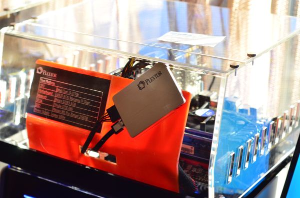
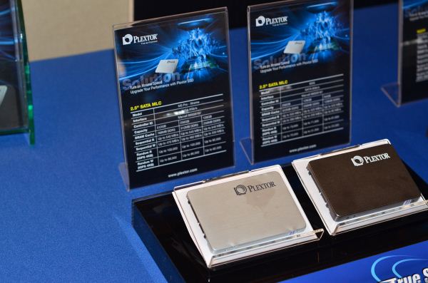
| 4:30p | Plextor Introduces M5 Pro Xtreme SSD
Shipping at the end of this month is Plextor's new M5 Pro Extreme SSD, an update to the M5 Pro that we reviewed not too long ago. The M5 Pro Extreme still uses Marvell's 88SS9187 controller with Plextor's own custom firmware. Plextor moved to Toshiba's 19nm 2bpc MLC NAND with 16KB page sizes as well as a brand new garbage collection alogithm to hopefully improve worst case performance (and performance consistency). While the previous forced GC algorithm would only kick in once free blocks dropped to 4%, the new algorithm will kick in starting at 10% free block count and increase in aggressiveness until the value hits 4%. The M5 Pro Xtreme will be available in 128GB, 256 and 512GB capacities: Plextor has enjoyed tremendous growth over the past year and is now apparently #2 in the world in PC client SSD shipments (excluding Apple) behind Samsung. Drives sold through OEM systems are usually sold under the LiteOn brand, while retail/etail drives fall under the Plextor brand. Gallery: Plextor Introduces M5 Pro Xtreme SSD  
| ||||||||||||||||||||||||||||||||||||||||||||||||||||||||||||||||||||||||||||||||||||||||||||||||||||||||||||||||||||||||||||||||||||||||||||||||||||||||||||||||||||||||||||||||||||||||||||||||||||||||||||||||||||||||||||||||||||||||
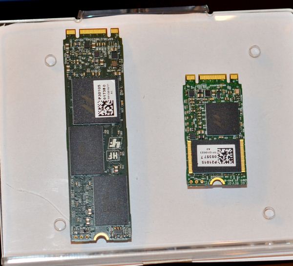
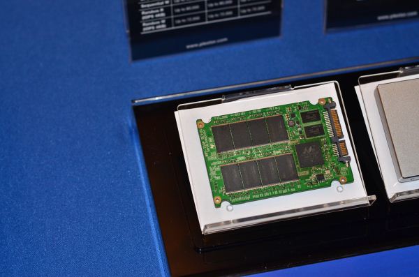
| 4:39p | Hands On with Plextor's NGFF SSDs
The Next Generation Form Factor for SSDs is designed to bring standardization to the wild west of Ultrabook SSD form factors. We reported on the standard at IDF, but in our Plextor meeting at CES we got the first look at two NGFF drives. The drive to the left uses Marvell's PCIe controller 88SS9183, while the smaller drive on the right is still 9187 based. Note that despite the difference in interface, both use the same connector. Both feature the new GC algorithm from the M5 Pro Xtreme. I also included a comparison to conventional mSATA drives so you can get an idea of the size reduction: You can expect both drives to be available by June of this year, with the SATA version coming in a couple months earlier.
Gallery: Hands On with Plextor's NGFF SSDs  
| ||||||||||||||||||||||||||||||||||||||||||||||||||||||||||||||||||||||||||||||||||||||||||||||||||||||||||||||||||||||||||||||||||||||||||||||||||||||||||||||||||||||||||||||||||||||||||||||||||||||||||||||||||||||||||||||||||||||||
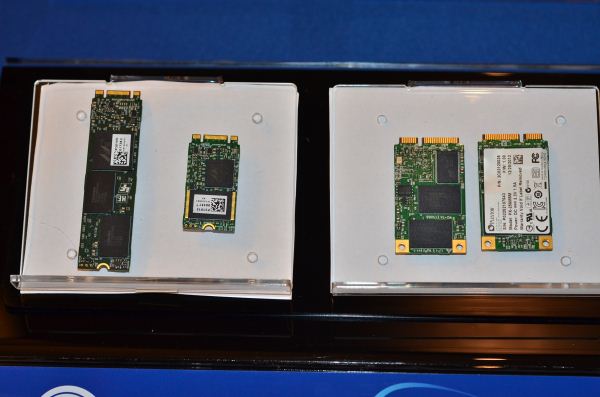
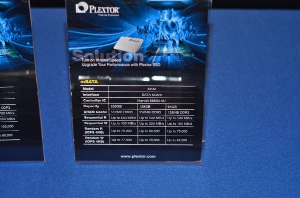
| 4:45p | Plextor's M5M mSATA SSD
In addition to the 2.5" SATA M5 Pro Xtreme, Plextor is bringing an mSATA version of the drive to market in the first half of this year as the M5M. The drive is architecturally identical to the M5 Pro Xtreme, with the same new firmware and Marvell controller, but it comes in a much smaller mSATA form factor. The M5M will be available in 64GB, 128GB and 256GB capacities, with performance that's a bit behind the M5 Pro Xtreme but still quite promising:
| ||||||||||||||||||||||||||||||||||||||||||||||||||||||||||||||||||||||||||||||||||||||||||||||||||||||||||||||||||||||||||||||||||||||||||||||||||||||||||||||||||||||||||||||||||||||||||||||||||||||||||||||||||||||||||||||||||||||||
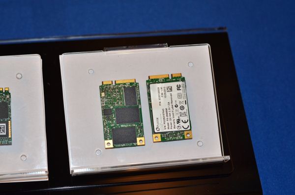
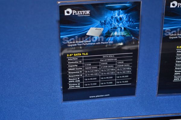
| 4:49p | Plextor's Dabbles in TLC NAND
Following in Samsung's footsteps, Plextor will be bringing a TLC version of its M5 series of SSDs to market towards the middle of the year. Despite the move to TLC NAND, Plextor is promising very good performance from the upcoming drive:
| ||||||||||||||||||||||||||||||||||||||||||||||||||||||||||||||||||||||||||||||||||||||||||||||||||||||||||||||||||||||||||||||||||||||||||||||||||||||||||||||||||||||||||||||||||||||||||||||||||||||||||||||||||||||||||||||||||||||||
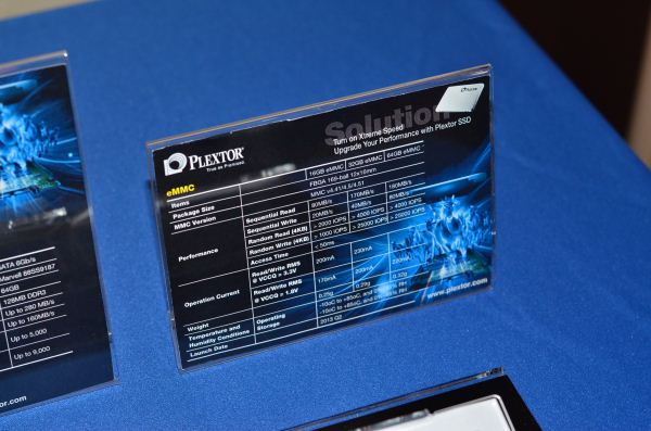
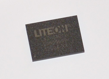
| 4:52p | Plextor/LiteOn Enters the eMMC Market
This is an unusual move but one that makes a lot of sense. Plextor is currently qualifing its first eMMC solution built around a Marvell controller. These integrated eMMC solutions are often found on tablets, unfortunately their performance tends to be pretty poor across the industry. Plextor hopes to change this with its solution and is promising sequential performance as high as 180/80MBps (writes/reads) and random write performance north of 25K IOPS. I have to say that I am happy to see some more competition here. Since this will be an OEM product it'll feature the LiteOn brand.
| ||||||||||||||||||||||||||||||||||||||||||||||||||||||||||||||||||||||||||||||||||||||||||||||||||||||||||||||||||||||||||||||||||||||||||||||||||||||||||||||||||||||||||||||||||||||||||||||||||||||||||||||||||||||||||||||||||||||||
| 5:01p | Razer Announces 10.1" Edge Gaming Tablet with Ivy Bridge, Kepler, Windows 8 We saw Razer's Project Fiona gaming tablet last year at CES, and came away from the hands-on opportunity and corresponding conversation with Razer CEO Min-Liang Tan fairly impressed with the device. It was chunky and hot, but it ran a Core i7 CPU and an unspecified Nvidia GPU. The concept still needed a fair amount of refinement, but it was clear that Razer had a fairly good idea there. This year at CES, Razer's big reveal is the Edge, essentially the production version of Project Fiona. It's a Windows 8 tablet running Core i5/i7 CPUs, an Nvidia GT 640M LE dGPU, and a 10.1" 1366x768 display. Like many of the new Windows 8 tablets, a lot of the story is hidden in the accessories and attachments - the Gamepad Controller being the most recognizable. Basically, the gaming controller/handles from Project Fiona are now part of a case that the tablet unit attaches into, with an optional extended battery that doubles battery life. Other accessories include a keyboard dock that uses a traditional keyboard and external mouse experience for MMO gamers and other heavily keyboard reliant games, as well as a docking station for connecting to big screens and external gamepads. From a hardware standpoint, the Edge is pretty interesting. The tablet unit comes in two different SKUs, regular and Pro. The regular comes with an unspecified Core i5 CPU, GT640M LE, 4GB DDR3, and a 64GB SSD for $999, while the Pro upgrades you to an i7, 8GB DDR3, and comes in 128GB and 256GB variants. Razer has not yet announced pricing for the Pro, but will be offering it in a bundle with the Gamepad Controller for presumably cheaper than the accessory on its own. The design of the Edge is pretty familar to anyone who has used the Blade. The back has the same radiused edges and contoured ridges on either side of a light-up Razer logo. Think of the Blade's lid scaled down to 10" and you've got a pretty good idea. Bet on a similar anodized aluminum unibody construction to the Blade. The front face is clean, with a single unbroken glass surface with a circular Windows button underneath the display and a webcam above. Ports and accessories on board include a single USB 3.0 port and Bluetooth 4.0. The dock/power connector is a rectangular slot-in kind, similar to the connector you see on the ASUS Transformer and VivoTab tablets. Now, there are a few interesting wrinkles here regarding the hardware: the odds that Razer is using one of the new 7W Ivy Bridge parts seems pretty high, there'd be no other way to fit a Core CPU and a midrange GPU, even a 28nm one, in a chassis of this size. There are a bunch of different GT 640M and GT640M LE SKUs, including some that are built on 40nm Fermi cores, but the Edge is virtually guaranteed to be using a 28nm Kepler part. And though it wasn't explicitly mentioned, I think Optimus graphics switching is a given. As far as SSD goes, a Marvell 88SS9174-based drive wouldn't be a bad bet, considering its use as the exclusive SSD controller in both generations of Blade, but I think I would lean towards it using the next-generation Marvell 88SS9187 controller. A major point of contention I have with the specs, on paper at least, has to do with the display. Razer specced a 10.1" 1366x768 TN panel for the Edge, and while I believe that this will be a high quality TN panel like that used on the Blade, I really have to question the decision to skip an IPS display. Razer's line is that the response rate of the IPS panels was not good enough, and while I think they believe that, I don't really agree with them. With these specs, you're going to be aiming for 40fps with any recent title, and we haven't seen any issues with IPS panels handling those kind of frame rates at all. I'm okay with the resolution though, GT640M LE will push 1366x768 displays pretty reasonably from a performance standpoint, while it'd probably choke and die at 1080p. Sure, you could play at lower-than-native resolution, but who wants to do that? That's a decision I understand, even if the panel type baffles me. I'll have a better idea of how the display actually is when I get my hands on with the Edge tomorrow. The Edge is a fairly thick tablet, at 0.8" thick it's about twice as thick as the fourth generation iPad and a solid amount thicker than the 0.53" Surface Pro. Weight, at 2lbs, is essentially the same as the Surface Pro though, which is not too bad. The footprint should be smaller due to the smaller display, though the bezel looks fairly large based on the press images. Now, the major reason the Edge needed to be so thick is simple: heat dissipation. To that end, there's also two pretty large vents at the top rear edge of the tablet. Large relative to the size of the body, at least. The chances of this tablet getting very hot are pretty high, particularly in gaming situations. Thankfully, if you're using the Gamepad Controller, you won't be holding the back of the tablet anyways, so it hopefully won't be as much of an issue. Obviously, throttling is a major issue to keep track of here, as is battery life when gaming. Razer says they've got some heat dissipation tricks up their sleeve here, a claim I'm more than happy to test out when I get my hands on one. Their thermal engineers have come up with some interesting solutions in the past, so I'm willing to believe them. Read on for a detailed discussion of the Edge accessories and pricing.
| ||||||||||||||||||||||||||||||||||||||||||||||||||||||||||||||||||||||||||||||||||||||||||||||||||||||||||||||||||||||||||||||||||||||||||||||||||||||||||||||||||||||||||||||||||||||||||||||||||||||||||||||||||||||||||||||||||||||||
| 6:00p | NVIDIA’s Annual GPU Rebadge Begins: GeForce GT 730M and GeForce 710M Partial Specs Published As we discussed yesterday with AMD’s latest round of GPU rebadges, both AMD and NVIDIA are locked into playing the OEM rebadge game in order to fulfill their OEM partner’s calendar driven schedules. OEMs want to do yearly updates (regardless of where the technical product cycle really is), so when the calendar doesn’t line up with the technology this is achieved through rebadges of existing products. In turn these OEMs put pressure on component suppliers to rebadge too, so that when consumers compare the specs of this year’s “new” model to last year’s model the former look newer. The end result is that both AMD and NVIDIA need to play this game or find themselves locked out of the OEM market. In any case, the bulk of these rebadges coincide with CES, which is where the OEMs announce their calendar-refresh products. We often see the specs for these systems leak out a couple of months in advance – and accordingly see the product numbers for the rebadged components they contain – but it’s not until CES that AMD and NVIDIA publish the specs of these products. So we’ve known these products were coming, we just haven’t had any solid details about them until now. Jumping right into things, this morning NVIDIA updated their GeForce product page with a link to a PDF with the specifications for two new mobile products: GeForce GT 730M and GeForce 710M. NVIDIA’s PDF doesn’t go into great detail – in particular they aren’t listing the clockspeeds at this time – but from the specs provided we can divine some more information about these first members of the 700M family.
For the time being we have a few unknowns and a few assumptions on our parts, but based on NVIDIA’s specs and naming scheme we are very confident about which GPUs are actually behind these products. The 730M is some kind of GK107 rebadge – almost certainly 640M – as evidenced by its support for Kepler family features such as TXAA, PCIe 3.0, and DisplayPort 1.2. We beiieve this to be 640M in particular based on the use of both GDDR5 and DDR3 and the product name, though a 650M rebadge is also a possibility due to the very similar features of those parts. The other part on NVIDIA’s current 700M series list is the GeForce 710M. This we believe to be a GF117 rebadge – almost certainly 620M – as evidenced by its lack of support for Kepler family features such as PCIe 3.0, TXAA, or support for resolutions over 2560x1600. This means that yes, just like the 600M series, the 700M series will contain some last-generation Fermi parts too, so any hope of a unified mobile family have been dashed by this product. Like the 620M this is a DDR3-only part, and exists as NVIDIA’s entry-level part over Intel’s iGPUs. It’s interesting to note that in lieu of clockspeeds (or really any other hard details) NVIDIA is listing something called the “GeForce Performance Score”, which is defined as the performance of the part relative to Intel’s HD4000 iGPU. The 730M and 710M are 4.8x and 3.0x respectively, and while NVIDIA is almost certainly being overgenerous in their performance estimations here, it does lend further proof to these being GK107 and GF117 rebadges. Finally, although NVIDIA has only published information on the 730M and 710M so far, based on previous experience we believe that this is only the tip of the iceberg. In the coming weeks (if not days) we would expect to see more mobile rebadges, along with some kind of desktop rebadge. We’ll keep our eyes peeled, so until they stay tuned.
| ||||||||||||||||||||||||||||||||||||||||||||||||||||||||||||||||||||||||||||||||||||||||||||||||||||||||||||||||||||||||||||||||||||||||||||||||||||||||||||||||||||||||||||||||||||||||||||||||||||||||||||||||||||||||||||||||||||||||


_575px.png)
_575px.png)
_575px.png)
| << Previous Day |
2013/01/08 [Calendar] |
Next Day >> |