[Most Recent Entries] [Calendar View]
Tuesday, January 7th, 2014
- Mantle
- AMD TrueAudio
- PCIe Gen 3
| Time | Event | ||||||||||||||||||||||||||||||||||||||||||||||||||||||||||||||||||||||||||||||||||||||||||||
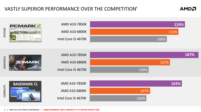
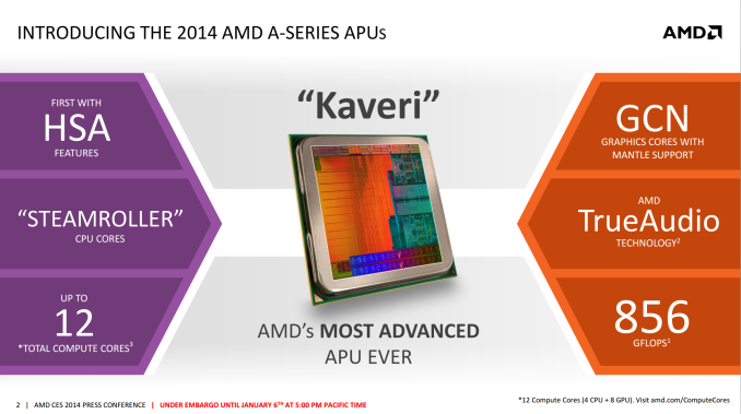
| 12:00a | AMD’s Kaveri: Pre-Launch Information On the back of AMD’s Tech Day at CES 2014, all of which was under NDA until the launch of Kaveri, AMD have supplied us with some information that we can talk about today. For those not following the AMD roadmap, Kaveri is the natural progression of the AMD A-Series APU line, from Llano, Trinity to Richland and now Kaveri. At the heart of the AMD APU design is the combination of CPU cores (‘Bulldozer’, ‘Steamroller’) and a large dollop of GPU cores for on-chip graphics prowess. Kaveri is that next iteration in line which uses an updated FM2+ socket from Richland and the architecture is updated for Q1 2014. AMD are attacking with Kaveri on four fronts: Redesigned Compute Cores* (Compute = CPU + GPU) Kaveri uses an enhanced version of the Richland CPU core, codename Steamroller. As with every new CPU generation or architecture update, the main goal is better performance and lower power – preferably both. AMD is quoting a 20% better x86 IPC with Kaveri compared to Richland when put clock to clock. For the purposes of this information release, we were provided with several AMD benchmarking results to share: These results border pretty much on the synthetic – AMD did not give any real world examples today but numbers will come through in time. AMD is set to release two CPUs on January 14th (date provided in our pre-release slide deck), namely the A10-7700K and the A10-7850K. Some of the specifications were also provided:
All the values marked ‘?’ have not been confirmed at this point, although it is interesting to see that the CPU MHz has decreased from Richland. A lot of the APU die goes to that integrated GPU, which as we can see above becomes fully GCN, rather than the Cayman derived Richland APUs. This comes with a core bump as well, seeing 512 GPU cores on the high end module – this equates to 8 CUs on die and what AMD calls ’12 Compute Cores’ overall. These GCN cores are primed and AMD Mantle ready, suggesting that performance gains could be had directly from Mantle enabled titles. Described in AMD’s own words: ‘A compute core is an HSA-enabled hardware block that is programmable (CPU, GPU or other processing element), capable of running at least one process in its own context and virtual memory space, independently from other cores. A GPU Core is a GCN-based hardware block containing a dedicated scheduler that feeds four 16-wide SIMD vector processors, a scalar processor, local data registers and data share memory, a branch & message processor, 16 texture fetch or load/store units, four texture filter units, and a texture cache. A GPU Core can independently execute work-groups consisting of 64 work items in parallel.’ This suggests that if we were to run asynchronous kernels on the AMD APU, we could technically run twelve on the high end APU, given that each Compute Core is capable of running at least one process in its own context and virtual memory space independent of the others. The reason why AMD calls them Compute Cores is based on their second of their four pronged attack: hUMA. HSA, hUMA, and all that jazz AMD went for the heterogeneous system architecture early on to exploit the fact that many compute intensive tasks can be offloaded to parts of the CPU that are designed to run them faster or at low power. By combining CPU and GPU on a single die, the system should be able to shift work around to complete the process quicker. When this was first envisaged, AMD had two issues: lack of software out in the public domain to take advantage (as is any new computing paradigm) and restrictive OS support. Now that Windows 8 is built to allow HSA to take advantage of this, all that leaves is the programming. However AMD have gone one step further with hUMA, and giving the system access to all the memory, all of the time, from any location: Now that Kaveri offers a proper HSA stack, and can call upon 12 compute cores to do work, applications that are designed (or have code paths) to take advantage of this should emerge. One such example that AMD are willing to share today is stock calculation using LibreOffice's Calc application – calculating the BETA (return) of 21 fake stocks and plotting 100 points on a graph of each stock. With HSA acceleration on, the system performed the task in 0.12 seconds, compared to 0.99 seconds when turned off. Prong 3: Gaming Technologies In a year where new gaming technologies are at the forefront of design, along with gaming power, AMD are tackling the issue on one front with Kaveri. By giving it a GCN graphics backbone, features from the main GPU line can fully integrate (with HSA) into the APU. As we have seen in previous AMD releases and talks, this means several things: AMD is wanting to revolutionize the way that games are played and shown with Mantle – it is a small shame that the Mantle release was delayed and that AMD did not provide any numbers to share with us today. The results should find their way online after release however. Prong 4: Power Optimisations With Richland we had CPUs in the range of 65W to 100W, and using the architecture in the FX range produced CPUs up to 220W. Techincally we had 45W Richland APUs launch, but to date I have not seen one for sale. However this time around, AMD are focusing a slightly lower power segment – 45W to 95W. Chances are the top end APUs (A10-7850K) will be 95W, suggesting that we have a combination of a 20% IPC improvement, 400 MHz decrease but a 5% TDP decrease for the high end chip. Bundle in some HSA and let’s get this thing on the road. Release Date AMD have given us the release date for the APUs: January 14th will see the launch of the A10-7850K and the A10-7700K. Certain system builders should be offering pre-built systems based on these APUs from today as well.
| ||||||||||||||||||||||||||||||||||||||||||||||||||||||||||||||||||||||||||||||||||||||||||||
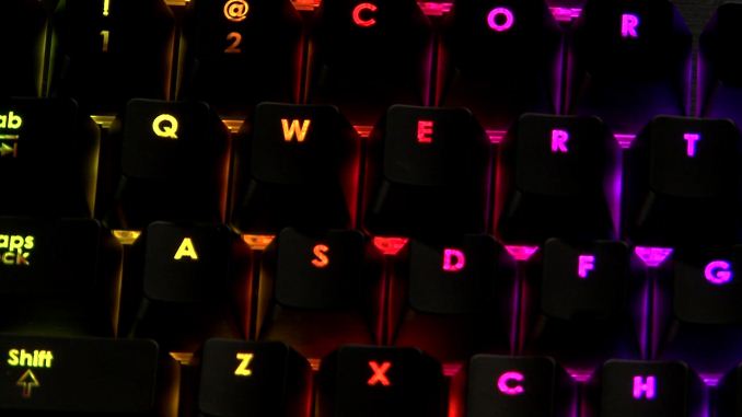
| 2:00a | Corsair at CES 2014: A Mechanical Keyboard with Per-Key Full RGB, aka the MX RGB Project
In a small CES preview, Corsair have emailed us about one of their internal design projects they will be showcasing this year at the Consumer Electronics Show in Las Vegas. Corsair is calling this the MX RGB Project: 100% mechanical key switches with per-key color backlighting, giving the user full control of 16.8 million color resolution. This is a collaboration between Corsair and Cherry Corp., a technical showcase based on a Vengeance K70 keyboard and new Cherry MX RGB switches. The aim is to get a similar product on the shelves in the second half of 2014 in the fast Cherry MX Red, the light tactile Cherry MX Brown, or tactile and audible Cherry MX Blue. Corsair wants feedback on ideas like this: I for one could see it useful for lighting up different keys that have different functions in different games. If it can detect when I am playing Battlefield 4 vs. Borderlands 2 or Grand Theft Auto, then I cannot wait to see it in the flesh. Expect it to be available sometime after Computex, when I am sure we will see a near-final version.
| ||||||||||||||||||||||||||||||||||||||||||||||||||||||||||||||||||||||||||||||||||||||||||||
| 7:00a | AMD Press Conference Highlights
Ian has already written up most of the information AMD covered in their press conference tonight, so if you haven’t already I suggest you start there. Kaveri is the big topic, but they also had plenty more to say about HSA and some of their other platforms, as well as demos of several systems and the current state of their “holodeck initiative” – complete with LaVar Burton (aka Geordi Leforge from Star Trek: TNG). I was without internet during the presentation so instead of a Live Blog I’m just going to post some comments on the highlights, as well as a bunch of images for the interested. The success of APUs was another point AMD stressed yet again, and they moved from there into a focus on their HSA initiative. TrueAudio was also mentioned along with Mantle, and AMD notes that there are currently three game engines in development with support for Mantle (Frostbite 3, Nitrous, and Asura), with five developers using Mantle in over twenty upcoming games. Battlefield 4 is the closest to release, and AMD demonstrated the Mantle version running on AMD hardware tonight, noting that the Mantle version is running 45% faster than the non-Mantle version on the same system. Other demonstrations included HSA/TrueAudio being used by Nuance to clean up audio streams to the point where they could do speech/voice recognition even in noisy environments. Libre Office noted a speedup of up to 8X with HSA acceleration enabled on a Kaveri A10-7850K vs. the same APU without HSA acceleration, though this was apparently with a huge spreadsheet. Kaveri is coming out on desktops next week with laptop versions to follow in Q2/Q3, as Ian discussed already. Beyond Kaveri AMD also has Beema and Mullins coming out in this year, with significant improvements in both CPU and GPU performance relative to Kabini and Temash; more importantly than the improvements relative to Kabini/Mullins, AMD had comparisons with Intel’s Bay Trail-T and Bay Trail-M. AMD is claiming Mullins performance 20% faster than Bay Trail-T in PCMark 8 Home and over 250% faster graphics performance in 3DMark11. Similarly, Beema performance is over 25% faster than Bay Trail-M in PDMark 8 Home and over 350% faster in GPU performance in 3DMark11. Even if we take those numbers with a healthy dose of skepticism, AMD is not surprisingly much faster than Intel on the GPU side, and they’re certainly competitive on the CPU side. AMD also announced a few design wins for Beema/Mullins tablets and laptops, with some desktop concepts shown as well. Gallery: AMD Press Conference Highlights _thumb.JPG) _thumb.JPG) _thumb.JPG) _thumb.JPG) _thumb.JPG) _thumb.JPG)
| ||||||||||||||||||||||||||||||||||||||||||||||||||||||||||||||||||||||||||||||||||||||||||||
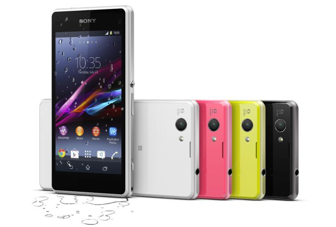
| 7:22a | Sony launches Xperia Z1 Compact, Z1S at CES 2014
Today at CES, Sony announced the Xperia Z1 Compact. This phone finally fills a slot that has been ignored in the Android device space, which is a phone that is easily used with one hand for the vast majority of people, and is also a high end flagship. While the Moto X also fits in this space, its SoC made it decidedly mid-high range, much like the Xperia S was at its debut. As always, specs are what determine where a product slots in the high/mid/low ranges, so it’s well worth going over them.
Sony also launched the Z1S, a variant of the Xperia Z1 for T-Mobile US. The only notable changes are for radio bands and a bump to 32GiB for internal storage. The Z1S will be available for preorder January 13th, with sales beginning on January 22nd. The Z1 Compact will go on sale globally in February.
| ||||||||||||||||||||||||||||||||||||||||||||||||||||||||||||||||||||||||||||||||||||||||||||
| 7:55a | Gigabyte’s New AORUS SLI Gaming Notebook
Gigabyte had all of their current generation notebooks on display, which you can see in the images below, but while many of them are interesting in their own right – and I like that all of them have either IPS or AHVA display panels as far as I could tell – the notebook that’s really aiming to garner a following is the new AORUS 17” notebook. Sporting two GTX 765M GPUs in SLI packed into a thin 22.9mm / 0.9” thick chassis that weighs 2.9kg / 6.39 lbs. the AORUS is aiming to take a crack at the slim gaming notebook market. It’s a daring design, and performance of the two 765M GPUs looks to be quite good. What’s more, the AORUS features three digital video outputs (two full-size HDMI and one mini-DP), allowing for three-screen surround gaming (and the fourth internal laptop display can continue to run as well). Build quality looks good as well, similar to that of the Razer Blade. Storage is handled by up to two mSATA SSDs in RAID 0 with a 2.5” HDD bay, along with four SO-DIMM slots allowing up to 32GB of RAM. Also present on the keyboard are five macro buttons with a toggle switch at the top providing access to 25 custom macros. Availability should be in the next quarter or two, and you can find additional details about the AORUS on the official site.
| ||||||||||||||||||||||||||||||||||||||||||||||||||||||||||||||||||||||||||||||||||||||||||||
| 1:40p | AMD/TI's DockPort Adopted As Official Extension to DisplayPort Standard
Shortly after the launch of Intel’s Thunderbolt interface in 2011, there was a great deal of discussion to be had in several camps over what the future of data and display interfaces may hold. Thunderbolt was a very intriguing interface, not only on a raw bandwidth basis but also on the basis of being able to reduce cable clutter by bringing data and display connectivity to a single small Mini DisplayPort connection. But with those capabilities came concern over the fact that Intel held exclusive control over the technology, and that its PCI-Express roots made the product more complex/expensive than what some manufacturers and system builders were willing to support. The end result was that a few different ideas were floated as potential Thunderbolt competitors. AMD’s Lightning Bolt proposal ended up being the frontrunner in this field, proposing a very Thunderbolt-like connection that would have USB 3.0 and power routed alongside DisplayPort, rather than Thunderbolt’s PCI-Express plus DisplayPort. However since AMD’s concept demo two years ago at CES 2012 we’ve heard very little about Lightning Bolt. Until today, that is. At CES 2014 the Video Electronics Standards Association (VESA) is announcing that Lightning Bolt, now operating under the name DockPort, is being adopted as an official extension to DisplayPort. This move effectively promotes DockPort from a 3rd party standard riding on top of DisplayPort to a 1st party standard that although not required for DisplayPort compliance, now has the backing of the entire VESA rather than just AMD and Texas Instruments. Equally important, like DisplayPort itself DockPort is going to be royalty free, opening the door for device makers and chip makers alike to implement it at-cost, without paying additional fees. With DockPort the VESA is initially targeting a slightly different series of use cases than what Intel and Apple have done with Thunderbolt, both for technical and pragmatic reasons. Whereas Thunderbolt is being used to supersede USB 3.0 in some cases, as DockPort is based on USB 3.0 there’s little need to supersede USB 3.0 as far as data connectivity is concerned. Rather DockPort will be focused on single-cable connectivity – and as implied by the DockPort name – as a docking interface for tablets and laptops. The latter in particular owing to the fact that DockPort carries power alongside its data and display components. As we’ve already seen with Thunderbolt products such as Apple’s Thunderbolt Display, there are definitely some good arguments to be had for offering a single combined data/display interface, as the continued shift from desktops to laptops has made monitors as docking stations an increasingly attractive option. Furthermore because DockPort provides power as well data, it should be possible to surpass Thunderbolt here and go truly single-cable on tablets and laptops, with the DockPort providing everything a laptop needs. However it remains unclear just how much power the standard will be able to provide to host devices, and consequently how big of a device can be powered through DockPort. Meanwhile on the technical side of matters, while there isn’t a final specification to have in hand quite yet (finalization is expected in the second quarter), DockPort looks very similar to AMD’s initial Lightning Bolt proposal. This means we’re looking at DisplayPort 1.2 with USB data multiplexed into the connection. DisplayPort 1.2 tops out at effective data rate of 17.2Gbps, with the DisplayPort display stream and the USB data stream sharing the connection. At the same time while DockPort cables won’t be identical to DisplayPort cables, the VESA has confirmed that DockPort will offer passive cables, allowing for DockPort cabling to be cheaper than the relatively expensive active cables that Thunderbolt requires. From a functionality perspective, due of the muxing of DisplayPort and USB the amount of bandwidth available to data devices will depend on in part the amount of bandwidth leftover after connected displays have consumed their share. Practically speaking this means that we expect AMD’s earlier claims to remain true, and that DockPort won’t be able to quite keep up with a native USB 3.0 connection. Meanwhile because this is USB based, this also means that manufacturers will be able to include just about any type of USB peripheral in their docks/monitors, including USB audio controllers, USB based NICs, and USB hubs, for all the benefits and drawbacks USB provides. Meanwhile in an interesting twist, due to the drawn out development of DockPort, the first DockPort controller is already out ahead of the specification itself. TI’s HD3SS2521 controller was unveiled back in 2013 when AMD and TI were still going it alone on DockPort, and is being used as the basis of the final standard. Until the standard is in hand it’s not clear quite how quickly DockPort devices will be available, but with TI already having a controller on the market the turnaround time should be much shorter than most other VESA standards (where the specification has come first and the silicon second). As for how widely DockPort will be adopted, it’s going to be a wait-and-see affair. Thunderbolt has seen little success outside of the Mac realm, and while the idea behind DockPort/Thunderbolt is very sound and useful, this doesn’t guarantee its adoption. Outright inertia carries a lot of weight in the PC industry and in the meantime plain DisplayPort is still relatively uncommon on laptops and mobile devices, especially outside of workstation grade laptops. On the other hand, having an open standard opens the doors to ultimately having multiple vendors with competing DockPort controllers, which offers the potential to keep controller costs closely in check. All the while the aforementioned passive cabling will bring down total costs even further. The use of USB instead of PCI-Express should also make DockPort more Windows-friendly than Thunderbolt, as USB is already hot-plug friendly as opposed to Thunderbolt requiring an additional layer of drivers to make PCI-Express behave properly with hot-plugging. Wrapping things up, AMD and TI will be showing off their initial work on DockPort at CES 2014, showcasing a version of the AMD Discovery concept tablet with DockPort functionality. Otherwise we should have more launch details on DockPort once the specification is finalized next quarter.
| ||||||||||||||||||||||||||||||||||||||||||||||||||||||||||||||||||||||||||||||||||||||||||||
| 2:00p | NVIDIA GeForce 332.21 WHQL Drivers Now Available
After November's s release of their 331.93 beta drivers, NVIDIA’s has pushed out another WHQL version of their R331 driver with today's release of driver version 332.21. As another iteration of the R331 series drivers, 332.21 is chiefly a bug fix and profile update driver. New SLI profiles have been added for Assetto Corsa, EVE Online (DX11), Plants vs. Zombies Garden Warfare, and Thief. Meanwhile this driver fixes several bugs, including a ShadowPlay resolution issue, browser crashes/freezes on Fermi GPUs, and issues with Microsoft Flight, Shadow Warrior, and Splinter Cell: Blacklist. As usual, you can grab the drivers for all current desktop and mobile NVIDIA GPUs over at NVIDIA’s driver download page.
| ||||||||||||||||||||||||||||||||||||||||||||||||||||||||||||||||||||||||||||||||||||||||||||
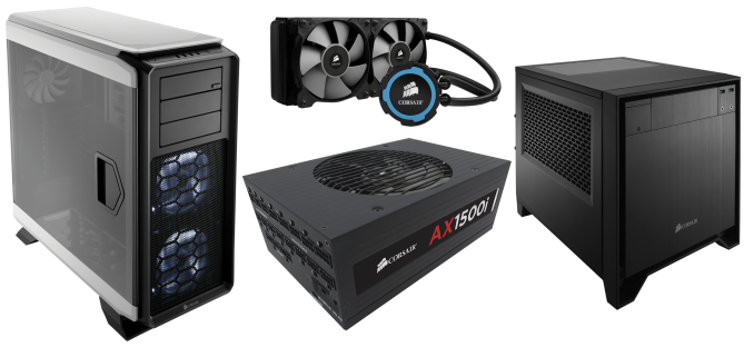
| 4:00p | Corsair Showcase a Technology Smörgåsbord at CES 2014
With another year comes another Consumer Electronics Show, held in Las Vegas every January. CES represents one of the three major showcasing events in the calendar, the other two being Computex held during June in Taiwan, and CeBIT held in Germany in March. Typically the North American and Asian shows hit hardest in terms of new releases and previews of upcoming equipment, and this year’s CES is no different. Corsair got in touch with us before the event regarding their new releases and previews, including new power supplies, cases, liquid cooling and keyboards. Here’s a sneak peak before we head on over to their booth.
| ||||||||||||||||||||||||||||||||||||||||||||||||||||||||||||||||||||||||||||||||||||||||||||
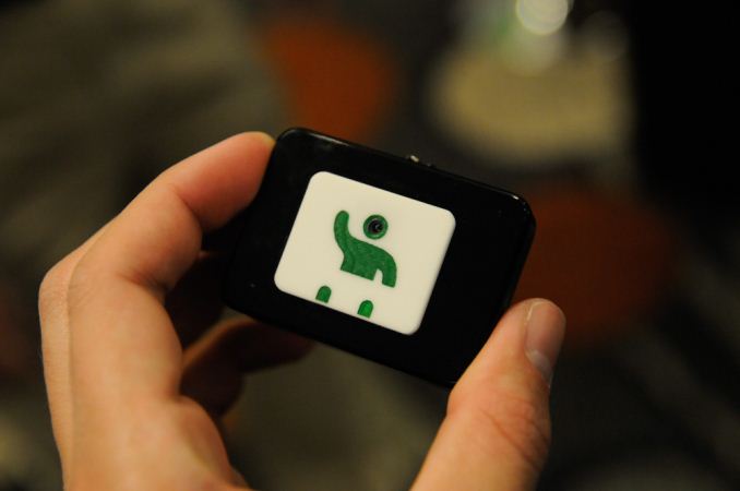
| 4:40p | Ambarella Shows off Wearable A7LW Camera Platform for Google Helpouts
Wearables seem to already be the unofficial theme of CES 2014, which officially begins today. I stopped by Ambarella to see their latest and greatest, now well known for making the SoC and video encode platform inside the popular GoPro series of cameras, which are based on the A7 and A7L SoCs. Ambarella was showing off a newly announced camera platform designed in a partnership with Google for Google Helpouts, a service designed to enable inscrutable sessions through what looks like the Google Hangouts interface, between a teacher and learner. The camera shown off is worn like a pendant, allowing the instructor to have full use of their hands while broadcasting and showing off whatever subject or task it is that they're instructing. There's a magnetic quick detach strap on the lanyard as well to allow the instructor to move the camera around as well. The goal is to make the platform easy to use as a secondary camera for Helpouts, and pairs either to a smartphone or tablet, or directly to a local WiFi AP. Video quality looked very good, with minimal latency, and battery life at 1080p30 is around 1.5 hours. There's no onboard storage since the application is streaming directly to the cloud, although the platform could easily support an SD card or eMMC. Ambarella expects partners to adopt the platform and make cameras designed specifically for Helpouts. The SoC is an A7L derivative called the A7LW (W for wearable) which consists of the same combination of ISP, video encoder up to H.264 High profile Level 5.0, 600 MHz ARM11 CPU, and built on a 32nm LP process, but further optimized for even lower power to squeeze it into wearables. Ambarella also noted that the A9 SoC which will enable 4Kp30 (UHD) encode and decode that we saw at CES 2013 (and again in a more final form at this CES playing back some new 4Kp30 content at 35 Mbps H.264) is now in production and that devices will arrive this year with it inside. Source: Ambarella
| ||||||||||||||||||||||||||||||||||||||||||||||||||||||||||||||||||||||||||||||||||||||||||||
| 5:19p | AnandTech Mobile Show at CES 2014 Today A couple of months ago Brian and I did a mobile show on video live from IDF where we discussed a lot of what was going on in mobile at the time. Intel was a huge help to us back then by providing support in the filming and production of the whole thing. It went over so well that Intel offered to help us out at CES this year to do the very same. This evening (at 6PM PT) Brian and I will be at Intel's booth at the Las Vegas Convention Center (Central Hall, Booth #7252) filming the second on-location AnandTech Mobile Show. We'll be discussing all of the mobile announcements at CES thus far, including the Tegra K1 that was just announced earlier this week. If you're at CES, feel free to drop by Intel's booth to check out the show as it's being filmed. We'll post the show to our YouTube channel immediately afterwards so look for it tomorrow evening. Update: It looks like we may get Intel's Hermann Eul (VP and GM of the Mobile & Comms group) to stop by for a candid interview on the show. This is going to be an exciting one. If there's anything you guys want us to discuss on the show let us know in the comments!
| ||||||||||||||||||||||||||||||||||||||||||||||||||||||||||||||||||||||||||||||||||||||||||||
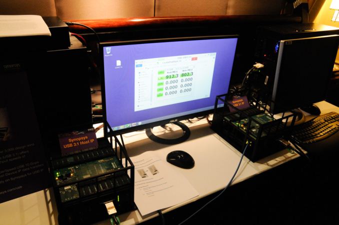
| 6:36p | USB-IF Updates Us on Type C Connector, Demonstrates USB SuperSpeed 3.1 Transfers
December of last year, the USB-IF announced that the definition of a new type of compact connector, dubbed type C, was underway. After pushback from the USB 3.0 micro-B connector, which added a lobe for the USB 3.0 data lines in addition to the signaling and port for USB 2.0 micro-B, many saw the definition of a type C connector as a way to learn from previous lessons and design a connector for better, sleeker industrial designs and with a new emphasis on mobile devices like tablets and smartphones. The type C connector is still in development, and there aren't any current renderings or drawings, but what has been laid out are the design goals for the new connector design. The connector will be reversible, and able to negotiation which end is host or client (direction-agnostic) with type c connectorization at both ends, although cables will still come in type-A to type-C combinations for use with power adapters and current generation hosts. In addition it will be around the same size as the current USB 2.0 Micro-B connector and catered toward enabling the kinds of thin and sleek industrial designs smartphone, tablet, and even notebook OEMs desire. Type C will work with USB 3.1 and the power delivery specification, in addition to including some extra pins for growth and building out the standard in the future, the goal is to make this the connector for the next 10 years. In addition, the standard will define an intermediary adapter for going from current 2.0 or 3.0 micro-B connectors to the new type C connector. I'm told to expect the Type C connector to have drawings and be better understood probably before the next IDF. In addition USB-IF showed two demos of USB 3.1, the new standard which enables up to 10 Gbps transfer speeds by doubling the clock rate and also moving to a more efficient 128b/132b coding scheme with just 3 percent overhead, compared to the 20% overhead in 10b/8b from USB 3.0. Both demos were implemented on FPGAs, and showed transfer rates right around 1 GB/s (8 Gbps), the second using Synopsis' FPGA implementation over current generation USB 3.0 cables.
| ||||||||||||||||||||||||||||||||||||||||||||||||||||||||||||||||||||||||||||||||||||||||||||


_575px.JPG)


_575px.JPG)
_thumb.JPG)
_thumb.JPG)
_thumb.JPG)
_thumb.JPG)
_thumb.JPG)
_thumb.JPG)


| << Previous Day |
2014/01/07 [Calendar] |
Next Day >> |