[Most Recent Entries] [Calendar View]
Tuesday, August 12th, 2014
- Completely new design but with backwards compatibility
- Similar to the size of USB 2.0 Micro-B (standard Smartphone charging cable)
- Slim enough for mobile devices, but robust enough for laptops and tablets
- Reversible plug orientation for ease of connection
- Scalable power charging with connectors being able to supply up to 5 A and cables supporting 3 A for up to 100 watts of power
- Designed for future USB performance requirements
- Certified for USB 3.1 data rates (10 Gbps)
- Receptacle opening: ~8.4 mm x ~2.6 mm
- Durability of 10,000 connect-disconnect cycles
- Improved EMI and RFI mitigation features
| Time | Event | ||||||||||||||||||||||||||||||||||||||||||||||||||||||||||||||||||||||||||
| 12:01a | Lenovo Announces New ThinkStation P Series Desktop Workstations
As much as I would like to be at SIGGRAPH, one of the reasons to visit would be to see Lenovo’s latest launch of their Haswell-E Desktop Workstation series. One of the key elements to the workstation market in recent quarters is to develop a professional-grade system that can encompass all the critical industries that require horsepower under the desk: engineering, media, energy, medical, finance and others. These systems have to be verified with industry standards to even be considered by these markets, but also the shift to Haswell-E and DDR4 will be an all-important factor for those that rely on speed and performance. One of the issues that these system manufacturers have is to define themselves in the market – Lenovo is already a big player in many other PC-related industries, so listening to customers is all important when trying to develop market share.
The new ThinkStation P series will be based around the LGA2011-3 socket, using Xeon processors and high capacity DDR4 memory. Given the nature of the platform, we can assume that the DDR4 will be ECC by default. For GPU Compute Quadro is being used, with the top line P900 model supporting dual Xeons alongside up to three Quadro K6000 graphics cards and up to 14 storage devices. All the P series will be certified to work on all key ISV applications, and via Intel they are quoted as supporting Thunderbolt 2, which should make for interesting reading regarding the PCIe lane distribution or PLX chip distribution depending if it is onboard or via an optional add-in-card. In terms of that all important product differentiation, the P series will use ‘tri-channel cooling’ and air baffles to direct the cool air immediately to the component in question and then out of the chassis without touching other components. This essentially becomes a more integrated solution than the compartmentalized chassis we see in the consumer market, except when the company makes the whole system, the company can control the experience to a much tighter level.
The P series also runs a trio of ‘FLEX’ themed additions. The FLEX Bay is designed to support an optical drive or the FLEX module which can hold an ultraslim ODD, media reader or firewire hub. The FLEX Tray on the P900 allows each of the seven HDD trays to support either one 3.5” drive or two 2.5” drives, hence the fourteen drive support mentioned earlier. The FLEX Connector is a mezzanine card allowing users to add in storage related cards without sacrificing rear PCIe slots, meaning that this connector brings this extra card away from the other devices, presumably at right angles. Lenovo is also wanting to promote their tool-less power supply removal without having to adjust the cables on the P700 and P500, which suggests that the PSU connects into a daughter PCB with all the connectors pre-connected, allowing the PSU to be replaced easily. Lenovo is also adorning their components with QR codes so if a user has an issue the code can be scanned such that the user will be directed to the specific webpage dealing with the component. The chassis will have integrated handles for easier movement or rack mounting. Lenovo is also promoting its diagnostic port, allowing the user to plug in an Android smartphone or tablet via USB for system analysis using the ThinkStation app.
Until Haswell-E and the motherboard chipsets are officially announced, Lenovo cannot unfortunately say more about the specifications regarding the series beyond memory capacities, DRAM support and power supply numbers, however they do seem confident in their ability to provide support and an experience to their ThinkStation users. We have been offered a review sample later in the year when we can test some of these features. Source: Lenovo
Addition: Ryan recently met with Lenovo last week where we were allowed to take some images of the chassis and design:
Gallery: Lenovo P-Series Event Photos
      | ||||||||||||||||||||||||||||||||||||||||||||||||||||||||||||||||||||||||||
| 6:00a | Browser Face-Off: Battery Life Explored 2014 It has been five years since we did a benchmark of the various web browsers and their effect on battery life, and a lot has changed. Our testing then included Opera 9 & 10, Chrome 2, Firefox 3.5.2, Safari 4, and IE8. Just looking at those version numbers is nostalgic. Not only have the browsers gone through many revisions since then, but computer hardware and the Windows operating system are very different. While there has been a lot of talk, there hasn't been a lot of data comparing browser battery usage. Today we're going to put the latest browsers to the test and deliver some concrete numbers. | ||||||||||||||||||||||||||||||||||||||||||||||||||||||||||||||||||||||||||
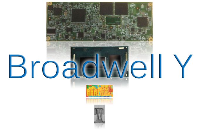
| 6:00a | Short Bytes: Intel's Core M and Broadwell-Y SoC
Intel has slowly been feeding us information about their upcoming Broadwell processors for a couple years now, with the first real details kicking off almost a year ago at IDF 2013. Since then, the only other noteworthy piece of information came back in March when it was revealed that socketed Broadwell CPUs with unlocked multipliers will be available with Iris Pro Graphics. Today, Intel is ready to begin providing additional information, and it starts with the Broadwell-Y processor, which Intel is now referring to as an SoC (System On Chip). We have an in-depth article on the subject, but for Short Bytes we want to focus on the bottom line: what does this mean for end users? The big news for Broadwell is that it will be the first 14nm processor available to the public, following on the success of Intel's 22nm process technology. Shrinking the process technology from 22nm to 14nm can mean a lot of things, but the primary benefit this time appears to be smaller chip sizes and lower power requirements. The first parts will belong to the Core M family of products, a new line catering specifically to low power, high mobility form factors (typically tablets and hybrid devices). With Core M, Intel has their sights set on the fanless computing market with sub-9mm thick designs, and they have focused on reducing power requirements in order to meet the needs of this market. This brings us to Broadwell-Y, the lowest power version of Broadwell and the successor to Haswell-Y and the codename behind the new Core M.
The reality of Intel's Y-series of processors is that they haven't been used all that much to date. Only a handful of devices used Haswell-Y (and even fewer used Ivy Bridge-Y), mostly consisting of 2-in-1 devices that can function as both a laptop and a tablet. For example, the base model Surface Pro 3 uses a Core i3-4020Y, and Dell's XPS 11 and certain Venue Pro 11 tablets also use Y-series parts; Acer, HP, Sony, and Toshiba also have some detachable hybrid devices with the extreme low power processors. Unfortunately, pricing on the Y-series is generally much higher than competiting solutions (i.e. ARM-based SoCs), and there have been criticisms of Intel's higher power requirements and lower overall battery life as well. Core M thus serves marketing needs as well as technical requirements: it replaces the Core i3/i5/i7 Y-series parts and gives Intel a brand they can market directly at premium tablets/hybrids. And in another move likely driven by marketing, Core M will be the launch part for Intel's new 14nm process technology. Transitions between process technology usually come every 2-3 years, so the 14nm change is a big deal and launching with their extreme low power part makes a statement. The key message of Broadwell is clear: getting into lower power devices and improving battery life is a critical target. To that end, Broadwell-Y probably won't be going into any smartphones, but getting into more premium tablets and delivering better performance with at least competitive battery life relative to other SoCs is a primary goal.
Compared to the Haswell-Y parts, Intel has made some significant advances in performance as well as power use, which we've covered elsewhere. The cumulative effect of the improvements Intel is bringing is that Broadwell-Y has a greater than 2X reduction in TDP (Thermal Design Power) compared to Haswell-Y. It also has a 50% smaller and 30% thinner package and uses 60% lower idle power. Intel points out that Broadwell-Y is set to deliver more than a 2X improvement in performance per Watt over Haswell-Y, though that's a bit more of a nebulous statement (see below). Many of the improvements come thanks to Intel's increased focus on driving down power requirements. Where previous Intel processors targeted laptops and desktops as the primary use case and then refined and adjusted the designs to get into lower power envelopes, with Broadwell Intel is putting the Y-series requirements center stage. The term for this is "co-optimization" of the design process, and these co-optimizations for Broadwell-Y are what allows Intel to talk about "2x improvements". But you need to remember what is being compared: Haswell-Y and Broadwell-Y. Broadwell parts in general will certainly be faster/better than the current Haswell parts – Intel doesn't typically "go backwards" on processor updates – but you shouldn't expect twice the performance at the same power. Instead, Broadwell-Y should offer better performance than Haswell-Y using much less power, but if you reduce total power use by 2X you could increase performance by 5% and still claim a doubling of performance per Watt. And that's basically what Intel is doing here. Intel estimates the core Broadwell architecture to be around 5% faster than Haswell at the same clocks; specifically, IPC (Instructions Per Cycle) are up ~5% on average. Similarly, changes and improvements to the graphics portion of the processor should deliver more performance at a lower power draw. Add in slightly higher clock speeds and you get a faster part than last generation that uses less power. These are all good improvements, but ultimately it comes down to the final user experience and the cost. Everywhere you go, people are increasingly using tablets and smartphones for many of their daily computing needs, and being left out of that market is the road to irrelevance. Core M (Broadwell-Y) is Intel's latest push to make inroads into these extremely low power markets, and on paper it looks like Intel has a competitive part. It's now up to the device vendors to deliver compelling products, as fundamentally the choice of processor is only one element of an electronics device. Being the first company to deliver 14nm parts certainly gives Intel an edge over the competition, but high quality Android and iOS tablets sell for $300-$500, so there's not a lot of room for a $100+ processor – which is why Intel has their Atom processors (due for the 14nm treatment with Braswell, if you're wondering). Core M is going after the premium tablet/hybird market, with benefits including full Windows 8 support, but will it be enough? If you're interested in such a device and you don't already own the Haswell-Y version, Core M products should deliver slimmer and lighter devices with improved battery life and better performance. Don't expect a 10" Core M tablet to deliver the same battery life as a 7" Android/iOS device (at least, not without a larger battery), since the display and other components contribute a lot to power use and Windows 8 has traditionally been far less battery friendly than Android; still, Core M tablets may finally match or perhaps even exceed the battery life of similarly sized iOS/Android tablets. The first retail products with Core M should be shipping before the end of the year, so we'll find out later this year and early next how well Broadwell-Y is able to meet its lofty goals. And we'll also find out how much the Core M products cost. | ||||||||||||||||||||||||||||||||||||||||||||||||||||||||||||||||||||||||||
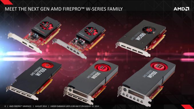
| 8:00a | AMD Completes FirePro Refresh, Adds 4 New FirePro Cards
Kicking off a busy day for professional graphics, AMD is first up to announce that they will be launching a quartet of new FirePro cards. As part of the company’s gradual FirePro refresh that began with the W9100 in April and followed by W8100 in June, today AMD is gearing up to refresh the rest of their FirePro lineup with new products for the mid-range and low-end segments of the pro graphics market. Being announced today are the FirePro W7100, W5100, W4100, and W2100. These parts are based on a range of AMD GPUs – including Tonga, a new GPU that has yet to show up in any other AMD products – and are designed to the sub-$2500 market segment that the current W8100 tops out at. With a handful of exceptions, the bulk of these upgrades are straightforward, focused on making AMD’s entire FirePro lineup 4K capable, improving performance across the board, and doubling the amount of VRAM compared to the past generation to allow for larger data sets to be used.
Starting at the top, from a technical perspective the W7100 is the most interesting of the new FirePro cards. Whereas the previous-generation W7000 was based on a second-tier version of AMD’s venerable Tahiti GPU, the W7100 gets a brand new GPU entirely, one that we haven’t seen before. Named Tonga, this new GPU is a smaller, lower performance GCN 1.1 part that slots in under the Hawaii GPU used in the W9100 and W8100. However while AMD is announcing the W7100 today they are not disclosing any additional information on Tonga, so while we can draw some basic conclusions from W7100’s specifications a complete breakdown of this new GPU will have to wait for another day.
From a specification point of view AMD is not disclosing the GPU clockspeed or offering any floating point throughput performance numbers, but we do know that W7100 will feature 1792 stream processors. Coupled with that is 8GB of GDDR5 clocked at 5GHz sitting on a 256-bit memory bus. The W7100 is designed to be a significant step up compared to the outgoing W7000. Along with the doubling W7000’s memory from 4GB to 8GB, the Tonga GPU in W7100 inherits Hawaii’s wider geometry front-end, allowing W7100 to process 4 triangles/clock versus W7000’s 2 tris/clock. Overall compute/rendering performance should also greatly be increased due to the much larger number of stream processors (1792 vs. 1280), but without clockspeeds we can’t say for sure. Like the W7000 before it, the W7100 is equipped with 4 full size DisplayPorts, allowing for a relatively large number of monitors to be used with the card. Because this is a GCN 1.1 GPU it gets the newer GCN 1.1 display controller, which for AMD’s 4K ambitions means that the monitor can drive 3 4K@60Hz displays or 4 4Kdisplays if some operate at 30Hz. In AMD’s product stack the W7100 is designed be a budget alternative to the W9100 and W8100, offering reduced performance but at a much lower cost. AMD is primarily targeting the engineering and media markets with the W7100, as its compute performance and 8GB of VRAM should be enough for most engineering workloads, or alternatively its VRAM capacity and ability to drive 4 4K displays makes it a good fit for 4K video manipulation.
The second card being introduced today is the W5100. This part is based on AMD’s Bonaire GPU, a GCN 1.1 GPU that has been in AMD’s portfolio for over a year now but has not made it into a FirePro part until now. W5100 replaces the outgoing W5000, which was a heavily cut-down Pitcairn part. In terms of specifications, the W5100 utilizes a slightly cut-down version of Bonaire with 768 SPs active. It is clocked at approximately 910MHz, which puts its compute performance at 1.4 TFLOPS for single precision. Feeding W5100 is 4GB of VRAM attached to a 128-bit memory bus and clocked at 6GHz. Compared to the outgoing W5000 the W5100 gains the usual VRAM capacity upgrades that the rest of the Wx100 cards have seen, while the other specifications are a mixed bag on paper. Compute performance is only slightly improved – from 1.28 TFLOPS to 1.4 TFLOPS – and memory bandwidth has actually gone regressed slightly from 102GB/sec. Consequently the biggest upgrade will be found in memory bound scenarios, otherwise the W5100’s greatest improvements would be from its GCN 1.1 lineage. Speaking of which, with 4 full size DisplayPorts the W5100 has the same 4K display driving capabilities as the W7100. However with lower performance and half the VRAM, it’s decidedly a mid-range card and AMD treats it as such. This means it’s targeted towards lower power usage scenarios where the high compute performance and 8GB+ VRAM capacities of the W7100 and higher aren’t needed.
The third of today’s new FirePro cards is the W4100. Based on AMD’s older Cape Verde GPU, this is not the first time that Cape Verde has appeared in a FirePro product. But it is the first time that it has appeared in a workstation part, its previous appearance being the display wall niche W600. At the same time the W4100 doesn’t have a true analogue in AMD’s previous generation FirePro stack, which stopped at the W5000, so the W4100 marks a newer, lower priced and lower performance tier for FirePro. With just 512 SPs active the W4100 tops out at only 50W power consumption, reflecting the fact that it is targeted towards lower power use cases. AMD has paired the card with 2GB of VRAM, and based on Cape Verde’s capabilities we expect that this is on a 128-bit bus. AMD has not provided any more technical details on the card, but it goes without saying that this is not a card meant to be a performance powerhouse. AMD’s target market for this is lightweight 2D and 3D workloads such as finance and entry level CAD. The 4 mini-DisplayPorts allow the card to directly drive up to 4 displays, though because this is a GCN 1.0 GPU it doesn’t have the same flexibility of the W5100.
The final FirePro card being introduced today is the FirePro W2100, which is AMD’s new entry-level FirePro card. Like the W4100 it had no true analogue in AMD’s older product stack, but functionally it replaces the old Turks based V4900, a card which AMD kept around even after the launch of GCN to serve as their entry level FirePro product. W2100 is based on AMD’s Oland GPU, which marks the first time that this existing AMD GPU has appeared in a FirePro product. W2100 uses a cut down version of Oland with 320 SPs active and attached to 2GB of memory on a 64-bit bus. Oland is a very limited functionality GPU, and while it’s more than suitable for basic imaging it should be noted that it doesn’t have a video decoder. At a TDP of just 26W, the W2100 is AMD’s lowest power, lowest performance card. Functionally it’s a cheaper alternative to the W4100 for users who don’t need to drive 4 displays, with W2100 featuring just 2 DisplayPorts. The targeted market is otherwise similar, with a focus on lightweight 2D and 3D workloads over 1-2 monitors.
Meanwhile along with today’s product announcements AMD is also announcing that they will be bringing their low-level Mantle API over to the FirePro family. The nature of the pro graphics market means that it will likely be some time before we see Mantle put in meaningful use here since the API is still under development, but once AMD gets the API locked down they believe that Mantle can offer many of the same benefits for professional graphics workloads as it can gaming. The greatly reduced draw call overhead should be a boon here for many 3D workloads, and Mantle’s ability to more easily transition between compute and graphics workloads would map well towards engineering tasks that want to do both at the same time. Wrapping things up, AMD has not revealed final pricing for these cards at this time, though we expect pricing to follow the previous generation W series cards. Meanwhile the W2100, W4100, and W5100 will be available next month. Otherwise no doubt owing to its use of the new Tonga GPU, W7100 will be farther out, with availability expected in Q4 of this year. | ||||||||||||||||||||||||||||||||||||||||||||||||||||||||||||||||||||||||||
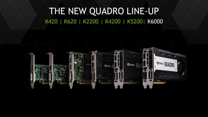
| 10:45a | NVIDIA Refreshes Quadro Lineup, Launches 5 New Quadro Cards
Continuing today’s spate of professional graphics announcements, along with AMD’s refresh of their FirePro lineup NVIDIA is announcing that they are undertaking their own refresh of their Quadro lineup. Being announced today and shipping in September are 5 new Quadro cards that will come just short of a top-to-bottom refresh of the Quadro lineup. With the exception of NVIDIA’s much more recently introduced Quadro K6000 – which will continue its reign as NVIDIA’s most powerful professional GPU – NVIDIA’s Quadro refresh comes as the bulk of the current Quadro K5000 family approaches 2 years old. At the point NVIDIA is looking to offer an across-the-board boost to their Quadro lineup, to increase performance and memory capacity at every tier. As a result this refresh will involve replacing NVIDIA’s Quadro cards with newer models based on larger and more powerful Kepler and Maxwell GPUs, and released as the Quadro Kx200 series. All told, NVIDIA is shooting for an average performance improvement of 40%, on top of any benefits from the larger memory amounts.
We’ll start things off with the Quadro K5200, NVIDIA’s new second-tier Quadro card. Based on a cut down version of NVIDIA’s GK110 GPU, the K5200 is a very significant upgrade to the K5000 thanks to the high performance and unique features found in GK110. The combination of which elevates the K5200 much closer to the K6000 than the K5000 it replaces.
The K5200 ships with 12 SMXes (2304 CUDA cores) enabled and utilizes a 256-bit memory bus, making this the first NVIDIA GK110 product we’ve seen ship without the full 384-bit memory bus. NVIDIA has put the GPU clockspeed at 650MHz while the memory clock stands at 6GHz. Meanwhile the card has the second largest memory capacity of the Quadro family, doubling K5000’s 4GB of VRAM for a total of 8GB. Compared to the K5000, K5200 offers an increase in shader/compute throughput of 36%, and a smaller 11% increase in memory bandwidth. More significant however are GK110’s general enhancements, which elevate K5200 beyond K5000. Whereas K5000 and its GK104 GPU made for a strong graphics card, it was a relatively weak compute card, a weakness that GK110 resolved. As a result K5200 should be similar to K6000 in that it’s a well-balanced fit for mixed graphics/compute workloads, and the ECC memory support means that it offers an additional degree of reliability not found on the K5000. As is usually the case in rolling out a refresh wave of cards based on existing GPUs, because performance has gone up power consumption has as well. NVIDIA has clamped K5200 at 150W (important for workstation compatibility), which is much lower than the full-fledged K6000 but is 28W more than the K5000. None the less the performance gains should easily outstrip the power consumption increase. Meanwhile display connectivity remains unchanged from the K5000 and K6000. NVIDIA’s standard Quadro configuration is a DL-DVI-I port, a DL-DVI-D port, and a pair of full size DisplayPorts, with the card able to drive up to 4 displays in total through a combination of those ports and MST over DisplayPort.
NVIDIA’s second new Quadro card is the K4200. Replacing the GK106 based K4000, the K4200 sees NVIDIA’s venerable GK104 GPU find a new home as NVIDIA’s third-tier Quadro card. Unlike K5200, K4200’s GPU shift doesn’t come with any kind of dramatic change in functionality, so while it will be an all-around more powerful card than the previous K4000, it’s still going to be primarily geared towards graphics like the K4000 and K5000 before it. For the K4200 NVIDIA is using a cut down version of GK104 to reach their performance and power targets. Comprised of 7 active SMXes (1344 CUDA cores), the K4200 is paired with 4GB of VRAM. Clockspeeds stand at 780MHz for the GPU and 5.4GHz for the VRAM. On a relative basis the K4200 will see some of the greatest performance gains of this wave of refreshes. Its 2.1 TFLOPS of compute/shader performance blasts past K4000 by 75%, and memory bandwidth has been increased by 29%. However the 4GB of VRAM makes for a smaller increase in VRAM than the doubling most other Quadro cards are seeing. Otherwise power consumption is once again up slightly, rising from 80W to 105W in exchange for the more powerful GK104 GPU. Finally, as was the case with K5200 display connectivity remains unchanged. Since the K4200 is a single slot card like K4000 before it, this means NVIDIA uses a single DL-DVI-I port along with a pair of full size DisplayPorts. Like other Kepler products the card can drive up to 4 displays, though doing this will require a DisplayPort MST hub to get enough outputs. Which on that note, users looking to pair this card with multiple monitors will be pleased to find that Quadro Sync is supported in the K4200 for the first time, being limited to the K5000 and higher previously. In NVIDIA’s refreshed Quadro lineup, the K4200 will primarily serve as the company’s highest-end single-slot offering. As with other GK10x based GPUs compute performance is not its strongest suit, while for graphics workloads such as CAD and modeling it should offer a nice balance of performance and price.
Moving on, NVIDIA’s third Quadro refresh card is the K2200. This replaces the GK107 based K2000 and marks the first Quadro product to utilize one of NVIDIA’s newest generation Maxwell GPUs, tapping NVIDIA’s GM107 GPU. The use of Maxwell on a Quadro K part makes for an amusing juxtaposition, though the architectural similarities between Maxwell and Kepler mean that there isn’t a meaningful feature difference despite the generation gap. As was the case with NVIDIA’s consumer desktop GM107 cards, NVIDIA is aiming to produce an especially potent sub-75W card for K2200. Here NVIDIA uses a fully enabled GM107 GPU – all 5 SMMs (620 CUDA cores) are enabled – and it’s paired with 4GB of VRAM on a 128-bit bus. Meanwhile based on NVIDIA’s performance figures the GPU clockspeed should be just north of 1GHz while the memory clock stands at 5GHz. Since the K2200 is replacing a GK107 based card, the performance gains compared to the outgoing K2000 should be significant. On the consumer desktop side we’ve seen GM107 products come close to doubling GK107 parts, and we’re expecting much the same here. K2200’s 1.3 TFLOPS of single precision compute/shader performance is 78% higher than K2000’s, which means that K2200 should handily outperform its predecessor. Otherwise the 4GB of VRAM is a full doubling over the K2000’s smaller VRAM pool, greatly increasing the size of the workloads K2200 can handle. Meanwhile display connectivity is identical to the new K4200 and the outgoing K2000. The K2200 can drive up to 4 displays by utilizing a mix of its DL-DVI port, two DisplayPorts, and a DisplayPort MST hub. In NVIDIA’s new Quadro lineup the K2200 will serve as their most powerful sub-75W card. As we’ve seen in other NVIDIA Maxwell products, this is an area the underlying GM107 excels at.
NVIDIA’s fourth Quadro card is the K620. This is another Maxwell card, and while NVIDIA doesn’t specify the GPU we believe it to be based on GM107 (and not GM108) due to the presence of a 128-bit memory bus. K620 replaces the GK108 based K600, and should offer substantial performance gains similar to what is happening with the K2200. K620’s GM107 GPU features 3 SMMs (384 CUDA cores) enabled, and it is pair with 2GB of DDR3 operating on a 128-bit memory bus. Like K2200 the GPU clockspeed appears to be a bit over 1GHz, and meanwhile the memory clockspeed stands at 1.8GHz. Compared to the K600 overall performance should be significantly improved. Though it’s worth pointing out that since memory bandwidth is identical to NVIDIA’s previous generation card, in memory bandwidth bound scenarios the K620 may not pull ahead by too much. None the less the memory pool has been doubled from 1GB to 2GB, so in memory capacity constrained situations the K620 should fare much better. Power consumption is just slightly higher this time, at 45W versus K600’s 41W. As this is a 3 digit Quadro product, NVIDIA considers this an entry level card and it is configured accordingly. A single DL-DVI port and a single full size DisplayPort are the K620’s output options, with an MST hub being required to attach additional monitors to make full use of its ability to drive 4 displays. By going with this configuration however NVIDIA is able to offer the K620 in a low profile configuration, making it suitable for smaller workstations that can’t accept full profile cards.
Finally, NVIDIA’s last new Quadro card is the K420. Dropping back to a Kepler GPU (likely GK107), it replaces the Quadro 410. From a performance perspective this card won’t see much of a change – the number of CUDA cores is constant at 192 – but memory bandwidth has been doubled alongside the total VRAM pool, which is now 1GB. Like K620, K420 can drive a total of 4 displays, while the physical display connectors are composed of a single DL-DVI port and a single full size DisplayPort. This low profile card draws 41W, the same as the outgoing 410.
With all but 1 of these cards receiving a doubled VRAM pool and significantly improved performance, NVIDIA expects that these cards should be well suited to accommodating the larger datasets that newer applications use, especially in the increasingly important subject of 4K video. Coupled with NVIDIA’s existing investment in software – both ISVs and their own cloud technology ecosystem – NVIDIA expects to remain ahead of the curve on functionality and reliability. Wrapping things up, NVIDIA tells us that the Quadro refresh cards will be shipping in September. In the meantime we’ll be reviewing some of these cards later this month, so stay tuned. | ||||||||||||||||||||||||||||||||||||||||||||||||||||||||||||||||||||||||||
| 12:00p | NVIDIA Launches Next GeForce Game Bundle - Borderlands: The Pre-Sequel
After letting their previous Watch Dogs bundle run its course over the past couple of months, NVIDIA sends word this afternoon that they will be launching a new game bundle for the late-summer/early-fall period. Launching today, NVIDIA and their partners will be bundling Gearbox and 2K Australia’s forthcoming FPS Borderlands: The Pre-Sequel with select video cards. This latest bundle is for the GTX 770 and higher, so buyers accustomed to seeing NVIDIA’s bundles will want to take note that this bundle is a bit narrower than usual since it doesn’t cover the GTX 760. As for the bundled game itself, Borderlands: The Pre-Sequel is the not-quite-a-sequel to Gearbox’s well received 2012 title Borderlands 2. As was the case with Borderlands 2 before it, this latest Borderlands game will be receiving PhysX enhancements courtesy of NVIDIA, leveraging the PhysX particle, cloth, and fluid simulation libraries for improved effects.
Meanwhile on a lighter note, it brings a chuckle to see that NVIDIA is bundling what will most likely be a Direct3D 9 game with their most advanced video cards. This if nothing else is a testament to longevity of the API, having long outlasted the hardware it originally ran on. Finally, as always, these bundles are being distributed in voucher from, with retailers and etailers providing vouchers with qualifying purchases. So buyers will want to double check whether their purchase includes a voucher for either of the above deals. Checking NVIDIA’s terms and conditions, the codes from this bundle are good through October 31st, so it looks like this will bundle will run for around 2 months. | ||||||||||||||||||||||||||||||||||||||||||||||||||||||||||||||||||||||||||
| 8:20p | Intel Disables TSX Instructions: Erratum Found in Haswell, Haswell-E/EP, Broadwell-Y
One of the main features Intel was promoting at the launch of Haswell was TSX – Transactional Synchronization eXtensions. In our analysis, Johan explains that TSX enables the CPU to process a series of traditionally locked instructions on a dataset in a multithreaded environment without locks, allowing each core to potentially violate each other’s shared data. If the series of instructions is computed without this violation, the code passes through at a quicker rate – if an invalid overwrite happens, the code is aborted and takes the locked route instead. All a developer has to do is link in a TSX library and mark the start and end parts of the code. News coming from Intel’s briefings in Portland last week boil down to an erratum found with the TSX instructions. Tech Report and David Kanter of Real World Technologies are stating that a software developer outside of Intel discovered the erratum through testing, and subsequently Intel has confirmed its existence. While errata are not new (Intel’s E3-1200 v3 Xeon CPUs already have 140 of them), what is interesting is Intel’s response: to push through new microcode to disable TSX entirely. Normally a microcode update would suggest a workaround, but it would seem that this a fundamental silicon issue that cannot be designed around, or intercepted at an OS or firmware/BIOS level. Intel has had numerous issues similar to this in the past, such as the FDIV bug, the f00f bug and more recently, the P67 B2 SATA issues. In each case, the bug was resolved by a new silicon stepping, with certain issues (like FDIV) requiring a recall, similar to recent issues in the car industry. This time there are no recalls, the feature just gets disabled via a microcode update. The main focus of TSX is in server applications rather than consumer systems. It was introduced primarily to aid database management and other tools more akin to a server environment, which is reflected in the fact that enthusiast-level consumer CPUs have it disabled (except Devil’s Canyon). Now it will come across as disabled for everyone, including the workstation and server platforms. Intel is indicating that programmers who are working on TSX enabled code can still develop in the environment as they are committed to the technology in the long run. Overall, this issue affects all of the Haswell processors currently in the market, the upcoming Haswell-E processors and the early Broadwell-Y processors under the Core M branding, which are currently in production. This issue has been found too late in the day to be introduced to these platforms, although we might imagine that the next stepping all around will have a suitable fix. Intel states that its internal designs have already addressed the issue. Intel is recommending that Xeon users that require TSX enabled code to improve performance should wait until the release of Haswell-EX. This tells us two things about the state of Haswell: for most of the upcoming LGA2011-3 Haswell CPUs, the launch stepping might be the last, and the Haswell-EX CPUs are still being worked on. That being said, if the Haswell-E/EP stepping at launch is not the last one, Intel might not promote the fact – having the fix for TSX could be a selling point for Broadwell-E/EP down the line. For those that absolutely need TSX, it is being said that TSX can be re-enabled through the BIOS/firmware menu should the motherboard manufacturer decide to expose it to the user. Reading though Intel’s official errata document, we can confirm this:
We are currently asking Intel what the required set of circumstances are to recreate the issue, but the erratum states ‘a complex set of internal timing conditions and system events … may result in unpredictable system behaviour’. There is no word if this means an unrecoverable system state or memory issue, but any issue would not be in the interests of the buyers of Intel’s CPUs who might need it: banks, server farms, governments and scientific institutions. At the current time there is no road map for when the fix will be in place, and no public date for the Haswell-EX CPU launch. It might not make sense for Intel to re-release the desktop Haswell-E/EP CPUs, and in order to distinguish them it might be better to give them all new CPU names. However the issue should certainly be fixed with Haswell-EX and desktop Broadwell onwards, given that Intel confirms they have addressed the issue internally. Source: Twitter, Tech Report
| ||||||||||||||||||||||||||||||||||||||||||||||||||||||||||||||||||||||||||
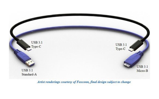
| 11:50p | USB Type-C Connector Specifications Finalized
Today it was announced by the USB-IF (USB Implementers Forum) that the latest USB connector which we first caught a glimpse of in April has been finalized, and with this specification many of the issues with USB as a connector should be corrected. USB, or Universal Serial Bus, has been with us for a long time now, with the standard first being adopted in 1996. At the time, it seemed very fast at up to 12 Mbps, and the connector form factor was not an issue on the large desktop PCs of the day, but over the years, the specifications for USB have been updated several times, and the connectors have also been updated to fit new form factor devices. In the early ‘90s, when USB was first being developed, the designers had no idea just how universal it would become. The first connectors, USB-A and USB-B, were not only massive in size, but the connection itself was only ever intended to provide power at a low draw of 100 mA. As USB evolved, those limitations were some of the first to go. First, the mini connectors were introduced, which, at approximately 3 mm x 7 mm, were significantly smaller than the original connector, but other than the smaller size they didn’t correct every issue with the initial connectors. For instance, they still had a connector which had to be oriented a certain way in order to be plugged in. As some people know, it can take several tries to get a USB cable to connect, and has resulted in more than a few jokes being made about it. The smaller size did allow USB to be used on a much different class of device than the original connector, with widespread adoption of the mini connectors on everything from digital cameras to Harmony remotes to PDAs of the day.
In January 2007, the Micro-USB connector was announced by the USB-IF, and with this change, USB now had the opportunity to become ubiquitous on smartphones and other such devices. Not only was the connector smaller and thinner, but the maximum charging rate was increased to up to 1.8 A for pins 1 and 5. The connection is also rated for at least 10,000 connect-disconnect cycles, which is much higher than the original USB specification of 1,500 cycles, and 5,000 for the Mini specification. However once again, the Micro-USB connector did not solve every issue with USB as a connector. Again, the cable was not reversible, so the cable must be oriented in the proper direction prior to insertion, and with USB 3.0 being standardized in 2008, the Micro connector could not support USB 3.0 speeds, and therefore a USB 3.0 Micro-B connector was created. While just as thin as the standard connector, it adds an additional five pins beside the standard pins making it a very wide connection. With that history behind us, we can take a look at the changes which were finalized for the latest connector type. There are a lot of changes coming, with some excellent enhancements: With this new design, existing devices won’t be able to mate using the new cables, so for that reason the USB-IF has defined passive cables which will allow older devices to connect to the new connector, or newer devices to connect to the older connectors for backwards compatibility. With the ubiquity of USB, this is clearly important.
There will be a lot of use cases for the new connector, which should only help cement USB as an ongoing standard. 10 Gbps transfer rates should help ensure that the transfer is not bottlenecked by USB, and with the high current draw being specified by connectors, USB may now replace the charging ports on many laptops as well as some tablets that use it now. The feature that will be most helpful to all users though is the reversible plug, which will finally do away with the somewhat annoying connection that has to be done today.
As this is a standard that is just now finalized, it will be some time before we see it in production devcies, but with the universal nature of USB, you can expect it to be very prevalent in upcoming technology in the near future.
| ||||||||||||||||||||||||||||||||||||||||||||||||||||||||||||||||||||||||||


| << Previous Day |
2014/08/12 [Calendar] |
Next Day >> |