[Most Recent Entries] [Calendar View]
Monday, August 18th, 2014
| Time | Event | ||||||||||||||||||||||||||||||||||||||||||||||||||||||||||||
| 6:00a | Browser Face-Off: Chrome 37 Beta Battery Life Revisited
Last week we posted our Browser Face-Off: Battery Life Explored 2014, where the battery run down times of Firefox 31, IE11 Desktop, IE11 Modern, Chrome 36, and Chrome 37 beta were tested on Windows. We used GUI automation to open browsers, tabs, and visit websites to simulate a real user in a light reading pattern. The article answered a lot of questions about popular browser battery life on Windows, but it raised additional questions as well.
When both Chrome 36 and Chrome 37 beta natively render at 1600x900 there is less than 3% difference in battery life. Two tests of each browser were performed and the results averaged. The variation between runs was only 1%. Looking at our previous numbers of Chome 36 and 37 beta on the HiDPI setting of 3200x1800 and 200% scaling, the situation is entirely different.
I've added an asterisk here (and clarified the same text on the original article) to indicate Chrome 36 isn't actually rendering at 3200x1800, but rather at 1600x900 and relying on Windows DPI Virtualization to scale up to 3200x1800. Looking at the numbers, we there's some good news and some bad news. The good news is that Chrome 37's new features likely won't hurt the battery life of current users. If you are using Chrome now, you are probably not using a HiDPI display due to the existing blurry rendering. For these users, the pending Chrome 37 upgrade has no significant impact on battery life. The bad news is that if you have been avoiding Chrome due to its HiDPI rending issues, Chrome 37 resolves those issues but also appears to provide worse battery efficiency compared to Internet Explorer. On our XPS 15 that equated to about an hour less of mobility. Given that this is the first version of Chrome to properly support HiDPI, it's entirely possible – even likely – that there are many opportunities to further optimize the algorithms and hopefully return battery life at least close to Chome 36 levels. A slight dip in battery life is expected as it takes more work to render a 3200x1800 image compared to a 1600x900 image, but a 20% drop seems rather extreme. We'll have to see what future updates bring, but hopefully by noting the discrepancy it will encourage developers to better tune performance. | ||||||||||||||||||||||||||||||||||||||||||||||||||||||||||||
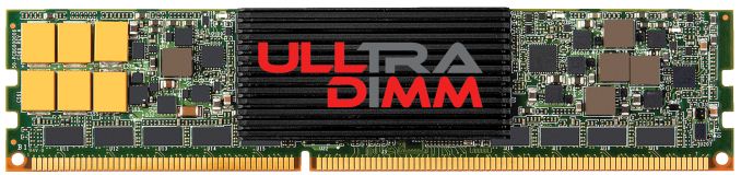
| 7:00a | FMS 2014: SanDisk ULLtraDIMM to Ship in Supermicro's Servers
We are running a bit late with our Flash Memory Summit coverage as I did not get back from the US until last Friday, but I still wanted to cover the most interesting tidbits of the show. ULLtraDIMM (Ultra Low Latency DIMM) was initially launched by SMART Storage a year ago but SanDisk acquired the company shortly after, which made ULLtraDIMM a part of SanDisk's product portfolio. The ULLtraDIMM was developed in partnership with Diablo Technologies and it is an enterprise SSD that connects to the DDR3 interface instead of the traditional SATA/SAS and PCIe interfaces. IBM was the first to partner with the two to ship the ULLtraDIMM in servers, but at this year's show SanDisk announced that Supermicro will be joining as the second partner to use ULLtraDIMM SSDs. More specifically Supermicro will be shipping ULLtraDIMM in its Green SuperServer and SuperStorage platforms and availability is scheduled for Q4 this year.
We have not covered the ULLtraDIMM before, so I figured I would provide a quick overview of the product as well. Hardware wise the ULLtraDIMM consists of two Marvell 88SS9187 SATA 6Gbps controllers, which are configured in an array using a custom chip with a Diablo Technologies label, which I presume is also the secret behind DDR3 compatibility. ULLtraDIMM supports F.R.A.M.E. (Flexible Redundant Array of Memory Elements) that utilizes parity to protect against page/block/die level failures, which is SanDisk's answer to SandForce's RAISE and Micron's RAIN. Power loss protection is supported as well and is provided by an array of capacitors.
The benefit of using a DDR3 interface instead of SATA/SAS or PCIe is lower latency because the SSDs sit closer to the CPU. The memory interface has also been designed with parallelism in mind and can thus take greater advantage of multiple drives without sacrificing performance or latency. SanDisk claims write latency of less then five microseconds, which is lower than what even PCIe SSDs offer (e.g. Intel SSD DC P3700 is rated at 20µs). Unfortunately there are no third party benchmarks for the ULLtraDIMM (update: there actually are benchmarks) so it is hard to say how it really stacks up against PCIe SSDs, but the concept is definitely intriguing. In the end, NAND flash is memory and putting it on the DDR3 interface is logical, even though NAND is not as fast as DRAM. NVMe is designed to make PCIe more flash friendly but there are still some intensive workloads that should benefit from the lower latency of the DDR3 interface. Hopefully we will be able to get a review sample soon, so we can put ULLtraDIMM through our own tests and see how it really compares with the competition. | ||||||||||||||||||||||||||||||||||||||||||||||||||||||||||||
| 9:00a | FMS 2014: HGST Announces FlashMAX III PCIe SSDs
Continuing with our Flash Memory Summit coverage, HGST announced their FlashMAX III enterprise SSD, which is the first fruit of HGST's Virident acquistion and continues Virident's FlashMAX brand. The FlashMAX III will come in half-height, half-length form factor and will be available in capacities of 1100GB, 1650GB and 2200GB. The controller is an FPGA-based 32-channel design with a PCIe 3.0 x8 interface, but there is no NVMe support since the FlashMAX III builds on the same architecture as the previous generation FlashMAX II.
The maximum throughput seems a bit low for a design that uses up eight PCIe 3.0 lanes since 2.7GB/s should be achievable with just four PCIe 3.0 lanes. Obviously performance scaling is not that simple but for example Samsung's XS1715 (which we will be reviewing soon!) is rated at up to 3.0GB/s while only consuming four PCIe 3.0 lanes. Using less PCIe lanes allows for more drives to be delpoyed as the amount of PCIe lanes is always rather limited. The 1650GB model is even slower due to the fact that it utilizes less NAND channels because it is a middle capacity. Basically, the 1100GB and 2200GB models have the same number of NAND packages, with the 2200GB model having twice as much NAND per package; the 1650GB model uses the higher capacity packages but doesn't fully populate the board. HGST told us that they are just testing the water to see if there is demand for something in between 1100GB and 2200GB. The FlashMAX III also supports Virident Flash-management with Adaptive Shceduling (vFAS), which is a fancy name for Virident's storage driver. vFAS presents the FlashMAX as a single volume block device to the OS, meaning that no additional storage protocols or controllers are needed, whereas some drives just use a RAID controller or need software RAID solutions to be configured into an array. Additionally vFAS handles NAND management by doing wear-leveling, garbage collection, data path protection, NAND-level parity, ECC, and more. The FlashMAX III is currently being qualified by select OEMs and will ship later in this quarter. | ||||||||||||||||||||||||||||||||||||||||||||||||||||||||||||
| 10:15a | NAS Units as VM Hosts: QNAP's Virtualization Station Explored Virtualization has been around since the 1960s, but it has emerged as a hot topic over the last decade or so. Despite the rising popularity, its applications have been mostly restricted to enterprise use. Hardware-assisted virtualization features (AMD-V, VT-x and VT-d, for example) have been slowly making their way into the lower end x86 parts, thereby enabling low-cost virtualization platforms. QNAP is, to our knowledge, the only NAS vendor to offer a virtualization platform (using the Virtualization Station package for QTS) with some of their units. Read on to find out how it works and the impact it has on regular performance. | ||||||||||||||||||||||||||||||||||||||||||||||||||||||||||||
| 8:10p | EVGA Torq X10 Gaming Mouse Review EVGA recently sent us their new Torq X10, a gaming mouse that also marks EVGA's first foray into the gaming peripheral market. On paper, it boasts excellent features and specifications. We are going to find out if it can live up to the high expectations of both the company and the consumers in this review. | ||||||||||||||||||||||||||||||||||||||||||||||||||||||||||||
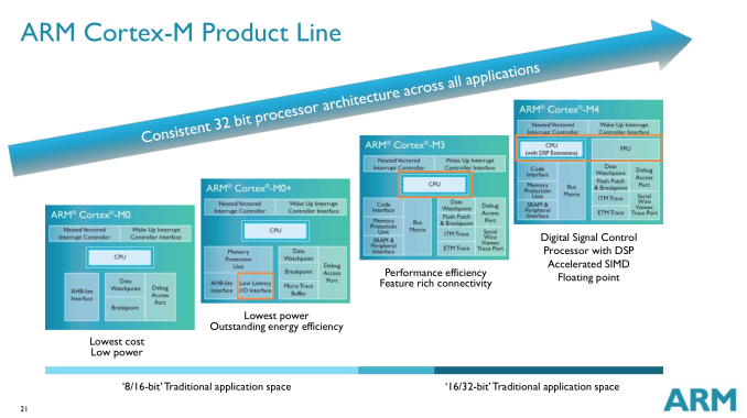
| 9:14p | ARM's Cortex M: Even Smaller and Lower Power CPU Cores
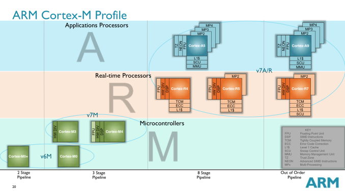
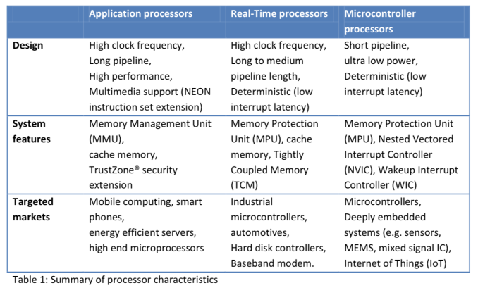
ARM (and its partners) were arguably one of the major causes of the present day smartphone revolution. While AMD and Intel focused on using Moore’s Law to drive higher and higher performing CPUs, ARM and its partners used the same physics to drive integration and lower power. The result was ultimately the ARM11 and Cortex A-series CPU cores that began the revolution and continue to power many smartphones today. With hopes of history repeating itself, ARM is just as focused on building an even smaller, even lower power family of CPU cores under the Cortex M brand. We’ve talked about ARM’s three major families of CPU cores before: Cortex A (applications processors), Cortex R (real-time processors) and Cortex M (embedded/microcontrollers). Although Cortex A is what we mostly talk about, Cortex M is becoming increasingly important as compute is added to more types of devices.
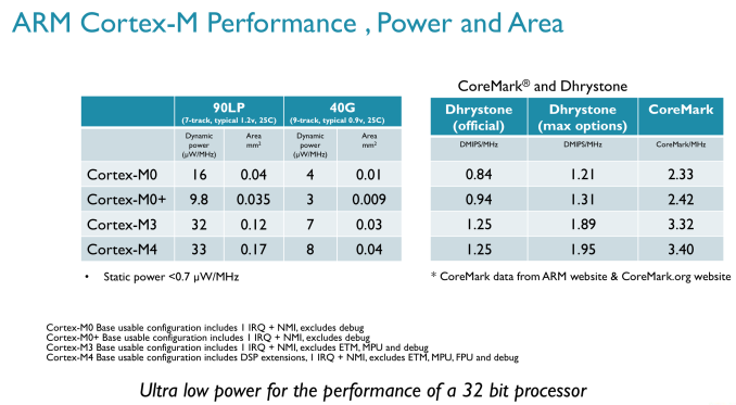
Wearables are an obvious fit for Cortex M, yet the initial launch of Android Wear devices bucked the trend and implemented Cortex A based SoCs. A big part of that is likely due to the fact that the initial market for an Android Wear device is limited, and thus a custom designed SoC is tough to justify from a financial standpoint (not to mention the hardware requirements of running Android outpace what a Cortex M can offer). Looking a bit earlier in wearable history and you’ll find a good number of Cortex M based designs including the FitBit Force and the Pebble Steel. I figured it’s time to put the Cortex M’s architecture, performance and die area in perspective. We’re very much in the early days of the evolution of Cortex M. The family itself has five very small members: M0, M0+, M1, M3 and M4. For the purposes of this article we’ll be focusing on everything but Cortex M1. The M1 is quite similar to the M0 but focuses more on FPGA designs. Before we get too far down the architecture rabbit hole it’s important to provide some perspective. At a tech day earlier this year, ARM presented this data showing Cortex M die area:
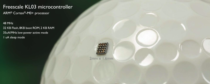
By comparison, a 40nm Cortex A9 core would be roughly around 2.5mm^2 range or a single core. ARM originally claimed the Cortex A7 would be around 1/3 - 1/2 of the area of a Cortex A8, and the Cortex A9 is roughly equivalent to the Cortex A8 in terms of die area, putting a Cortex A7 at 0.83mm^2 - 1.25mm^2. In any case, with Cortex M we’re talking about an order of magnitude smaller CPU core sizes. The Cortex M0 in particular is small enough that SoC designers may end up sprinkling in multiple M0 cores in case they need the functionality later on. With the Cortex M0+ we’re talking about less than a hundredth of a square millimeter in die area, even the tightest budgets can afford a few of these cores. In fact, entire SoCs based on Cortex M CPU cores can be the size of a single Cortex A core. ARM provided this shot of a Freescale Cortex M0+ design in the dimple of a golf ball:
ARM wouldn’t provide me with comparative power metrics for Cortex M vs. Cortex A series parts, but we do have a general idea about performance:
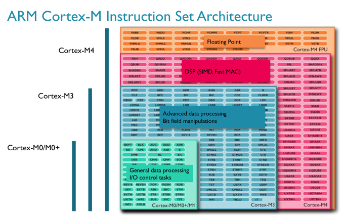
In terms of DMIPS/MHz, Cortex M parts can actually approach some pretty decent numbers. A Cortex M4 can offer similar DMIPS/MHz to an ARM11 (an admittedly poor indicator of overall performance). The real performance differences come into play when you look at shipping frequencies, as well as the type of memory interface built around the CPU. Cortex M designs tend to be largely SRAM and NAND based, with no actual DRAM. You'll note that the M3/M4 per clock performance is identical, that's because the bulk of what the M4 adds is in the form of other hardware instructions not measured by Dhrystone performance. Instruction set compatibility varies depending on the Cortex M model we’re talking about. The M0 and M0+ both implement ARM’s v6-M instruction profile, while the M3 and M4 support ARM’s v7-M. As you go up the family in terms of performance you get access to more instructions (M3 adds hardware divide, M4 adds DSP and FP instructions):
Each Cortex M chip offers a superset of the previous model’s instructions. So a Cortex M3 should theoretically be able to execute code for a Cortex M0+ (but not necessarily vice versa). You also get support for more interrupts the higher up you go on the Cortex M ladder. The Cortex M0/M0+ designs support up to 32 interrupts, but if you move up to the M3/M4 you get up to 240. All Cortex M processors have 32-bit memory addressability and the exact same memory map across all designs. ARM’s goal with these chips is to make moving up between designs as painless as possible. While we’ve spent the past few years moving to out-of-order designs in smartphone CPUs, the entire Cortex M family is made up of very simple, in-order architectures. The pipelines themselves are similarly simplified:
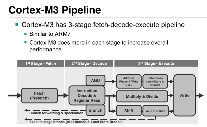
Cortex M0, M3 and M4 all feature 3-stage in-order pipelines, while the M0+ shaves off a stage of the design. In the 3-stage designs there’s an instruction fetch, instruction decode and a single instruction execute stage. In the event the decoder encounters a branch instruction, there’s a speculative instruction fetch that grabs the instruction at the branch target. This way regardless of whether or not the branch is taken, the next instruction is waiting with at most a 1 cycle delay. These aren’t superscalar designs, there’s only a 1-wide path for instruction flow down the pipeline and not many execution units to exploit. The Cortex M3 and M4 add some more sophisticated units (hardware integer divide in M3, MAC and limited SIMD in M4), but by and large these are simple cores for simple needs. The range of operating frequencies for these cores is relatively low. ARM typically expects to see Cortex M designs in the 20 - 150MHz range, but the cores are capable of scaling as high as 800MHz (or more) depending on process node. There’s a corresponding increase in power consumption as well, which is why we normally see lower clocked Cortex M designs.
Similar to the Cortex A and R lines, the Cortex M family has a roadmap ahead of it. ARM recently announced a new CPU design center in Taiwan, where Cortex M based cores will be designed. I view the Cortex M line today quite similarly to the early days of the Cortex A family. There’s likely room for a higher performing option in between Cortex M4 and Cortex A7. If/when we get such a thing I feel like we may see the CPU building block necessary for higher performance wearable computing. | ||||||||||||||||||||||||||||||||||||||||||||||||||||||||||||


_575px.png)
| << Previous Day |
2014/08/18 [Calendar] |
Next Day >> |