[Most Recent Entries] [Calendar View]
Friday, August 22nd, 2014
| Time | Event | ||||
| 6:00a | Recovering Data from a Failed Synology NAS It was bound to happen. After 4+ years of running multiple NAS units 24x7, I finally ended up with a bricked NAS. Did I lose data? Were my recovery attempts successful? If so, what sort of hardware and software setup did I use? How can you prevent something like that from happening in your situation? Read on to find out. | ||||
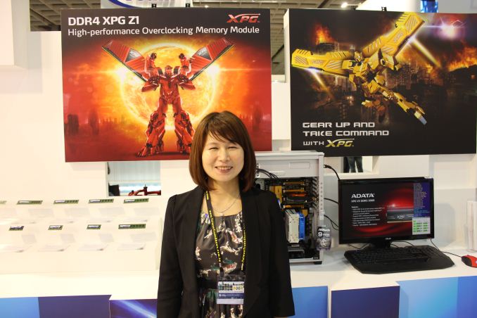
| 10:00a | Interview with ADATA's President Shalley Chen
At this year’s Computex, I had the opportunity to sit down with Mrs. Shalley Chen, ADATA’s President, to discuss the current trends in the memory and SSD business, as well as get an overview of ADATA’s future plans. Mrs. Chen has been with ADATA since the company was founded in 2001 and is also the wife of the founder, Simon Chen. Before stepping in as President in April this year, Mrs. Chen served as an Executive Vice President. Mrs. Chen also holds a degree in business management from the Ming Chuan University in Taiwan. Before we get into the actual interview, I want to provide a brief overview of ADATA. The company generates over $1 billion in yearly revenue, which makes ADATA one of the largest memory companies in the world. Over a half of the revenue comes from the APAC (Asia-Pacific) region, which is logical given ADATA’s Taiwanese roots and the size of the Asian market. The North and Latin America region ranks as the second largest revenue source with about 15% share in total revenue, followed by Europe and other smaller regions. In the interview Mrs. Chen hinted that Asia, Europe and especially Russia are potential future growth areas for ADATA since the memory and SSD markets are still in a developing stage, whereas in the US the markets are more mature. ADATA has had an office in the US since 2002 and employs 41 people across two offices in Los Angeles and Miami. These are both sales and customer support offices with the LA office in charge of North America while the Miami office is responsible for Latin America. All R&D is done in Taiwan at ADATA HQ whereas production is split between ADATA’s owned factories in China and Taiwan. While in Taiwan I took advantage of the offer to visit ADATA’s headquarters and the Taiwanese factory, as well as take some images for another article. Ever since the company was founded, ADATA has been a memory centric company. Like many companies of a similar nature, the mission, as it stood from day one, is to become the global leading brand of memory products. Although the product portfolio has grown over the years to include newer products such as USB flash drives, external hard drives, SSDs, memory cards, and, more recently, mobile power banks - fundamentally ADATA is still a memory company. Over half of ADATA’s revenue is generated by DRAM sales, and market researches rank ADATA as the Number Two DRAM module supplier in the world. Given the high competition in the memory and SSD business, the question I always put to the manufacturers is this: what differentiates you from all the other brands? There are a dozen consumer focused DRAM companies, and there is little room for innovation or differentiation in the industry. Mrs. Chen told me that ADATA’s best weapon against the competition starts from the diversity of the product portfolio to the close relations with both chip suppliers and distributors. Mrs. Chen was keen to point out that ADATA makes products for all three major markets (client, enterprise and industrial), giving ADATA several different revenue sources, and the percentage of revenues from enterprise and industrial is getting bigger and bigger. This directly implies that the enterprise and industrial segments are substantial to ADATA. Big enterprise OEMs like Intel and Samsung are typically interested only in large enterprises that buy upwards of tens of thousands of units, which leaves the small to medium size enterprise market to OEMs like ADATA to fight for the rest of the market. For example, some of Samsung’s enterprise products are only available to large OEMs (like EMC, Dell etc.), which leaves a niche for OEMs like ADATA and other smaller OEMs to offer better support for small to medium size enterprises. This also lends a benefit to work directly with the OEM for any customization. Like other fabless DRAM and SSD manufacturers, ADATA does not manufacture the chips they use – ADATA have to buys them from the likes of Micron and Samsung. I asked if ADATA has ever thought about moving to chip fabrication, but the answer was negative. The main reason is the cost of a fab, and investing billions of dollars is a large risk. If we look at the major semiconductor fabricators, most of them have been in the industry for decades, developing new technologies as the research progresses. As a result, it would be extremely difficult for a new player to gain any significant market share without innovation or a wide product portfolio and mountains of investment (it is worth noting that innovation can come from start-ups that have new technology but get acquired). Another point ADATA raised is that it has close relations with DRAM and NAND suppliers, and thus has no need for a chip fab. In the end, the DRAM module industry is all about managing inventory against cost and potential sales, so the competitive advantage lies in forecasting the demand and managing the inventory efficiently. The same applies to SSD controller development. Even though controllers can be fabricated by a third party, the capital required for the development and manufacturing is still a large sum. ADATA raised STEC as an example, which took the path to design its own controller platform but got into serious financial trouble due to the cost of the development. STEC ended up being acquired by Western Digital. ADATA does, however, have its own SSD firmware development team that has been in action since 2007. ADATA believes that the firmware team will play a key role to ensure competitiveness in the future. At this point in time, the team is mainly focusing on industrial SSD firmware development but there will be a change towards more unique firmware in the consumer side as well. One of the big topics at Computex was the state of DDR4, and ADATA was heavily presenting its DDR4 portfolio at the show. Given ADATA’s position, the company wants to be the leader in DDR4 and will aim to push the new technology quite aggressively to both consumers and enterprises. ADATA is one of Intel’s six Haswell-E/X99 launch partners (the others are Micron, Samsung, Hynix, Kingston and Crucial), so there should be plenty of ADATA DDR4 available when the X99 platform launches later this year. I asked ADATA whether the market for DDR4 will any different from current DDR3 from an OEM perspective. Mrs. Chen replied that DDR4 is different in the sense that right now DDR4 is mostly an enterprise product and will be sold through B2B marketing. The enterprise segment, due to the demand of more units per sale, also gets a greater benefit from DDR4, which is due to the lower voltage and higher frequency. The stereotypical scenario of hundreds of racks with each server equipped with eight to sixty-four DIMMs or more, lower power consumption on one module adds up and is thus always welcome. The speed should help enterprise workloads due to the tendency to be more often bound by memory performance than client workloads. For the end-users, ADATA showed us there will be branded products at retail as well, but until the mainstream platform adopts DDR4, the enterprise segment will be the main market. In terms of production, ADATA believes that DDR4 will overtake DDR3 in H1’15 for the enterprise market, but the same will not happen in the consumer side until sometime in 2016. All in all, there is a lot going on in both DRAM and SSD industries at the moment, so it will be interesting to see how the market reacts. We would like to thank Mrs. Chen and ADATA for their time giving us the opportunity to discuss the DRAM and SSD markets. As part of my visit to ADATA, I also met with ADATA’s DRAM and SSD directors to discuss their technology at a lower level. Keep your eyes peeled for that article in due course. | ||||
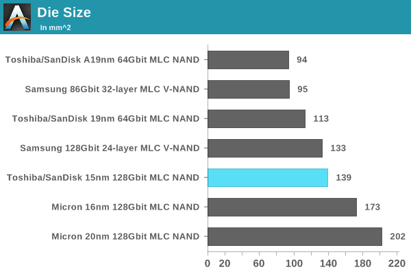
| 12:42p | Measuring Toshiba's 15nm 128Gbit MLC NAND Die Size
Courtesy of Custom PC Review At Flash Memory Summit, Toshiba was showcasing their latest 15nm 128Gbit MLC NAND wafer that has been developed in partnership with SanDisk. I simply could not resist to calculate the die size as Toshiba/SanDisk has not published it and die size is always the basis of any semiconductor cost analysis. Unfortunately I was too busy running between meetings that I did not take a photo of the wafer, so I am borrowing the picture from Custom PC Review.
To estimate the die size, I used the same method as with Samsung's second generation V-NAND. Basically I just calculated the amount of dies in both X and Y axes of the wafer as that gives as an approximation of the die size since we know that the diameter of the wafer is 300mm.
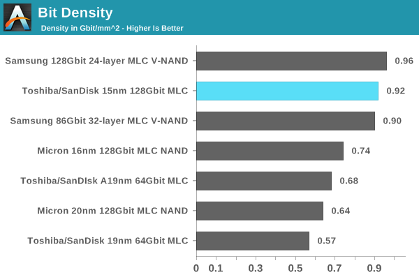
The 15nm node from Toshiba/SanDisk is extremely competitive. Its bit density is essentially equivalent to Samsung's V-NAND, so it is no wonder that Toshiba and SanDisk are betting heavily on their 15nm node before moving to 3D in early 2016. Compared to other 2D NAND dies, the 15nm node is a clear winner from bit density standpoint as Micron's 16nm MLC does not even come close.
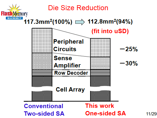
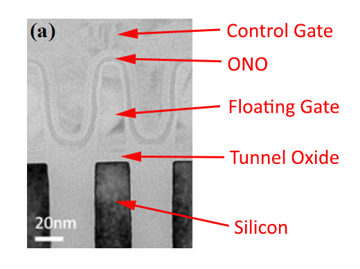
Toshiba's and SanDisk's secret lies in two-sided sense amp and all bit line (ABL) architecture, which reduce the size of the peripheral circuits and sense amplifier, resulting in higher memory array efficiency. Based on my estimation, the array efficiency (i.e. how big portion of the die is dedicated to memory cells) is about 80%, which is typical for a 128Gbit capacity. Higher capacities tend to yield better array efficiency since the peripheral circuitry does not scale as well as the memory cells do, so increasing the die capacity is one of the key solutions in lowering the cost per gigabyte.
Since nobody has yet taken a cross-section of the 15nm die, it is hard to say for sure what Toshiba and SanDisk are doing to shrink the dimensions. There is no mention of high-K dielectrics, so that seems unlikely and if history is any guidance, then Toshiba/SanDisk is simply increasing the aspect ratio by making the floating gate taller to compensate for the smaller feature size and keep the overall floating gate volume similar. That also helps to maintain the gate coupling ratio because the control gate is still wrapped around the floating gate and with a taller floating gate the capacitance between the gates should remain sufficient despite the increasing proximity of the floating gates. The production of Toshiba/SanDisk 15nm NAND node is currently ramping up and SSDs based on the new node are expected in Q4'14. | ||||
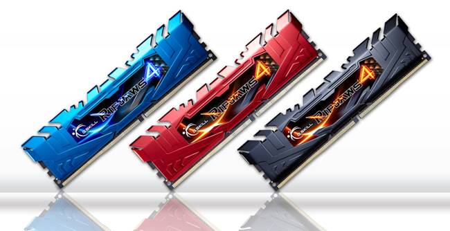
| 2:19p | G.Skill Announces Ripjaws DDR4, up to DDR4-3200
Much like the recent swathe of X99 motherboard previews we have seen, memory manufacturers are getting on board with showcasing their DDR4 memory modules to use with the Haswell-E platform. Unlike the CPUs from Intel, there is no formal NDA as such, allowing the media to report the design and specifications, although because real-world performance requires the CPU, no-one is able to post benchmark numbers. The new DDR4 from G.Skill is the next DRAM module manufacturer to come out with an official press release, and following the previous high performance Ripjaws DDR3 range G.Skill will introduce its memory under the Ripjaws 4 moniker with a new heatspreader design.
G.Skill’s press release confirms the voltage ranges for DDR4, with 1.2 volts being standard on 2133 MHz to 2800 MHz kits, with the higher performance modules at ≥3000 MHz and above requiring 1.35V. The product line that G.Skill is aiming to release at launch is quite impressive with all the 1.2 volt modules in 16GB, 32GB and 64 GB kits. Due to the extra binning and higher tolerances of the more performance oriented kits, the DDR4-3000 C15 will be in 16GB or 32GB kits, DDR4-3000 C16 will be in a kit 32GB and the top line 3200 MHz C16 will be in a 16GB kit only.
G.Skill is reporting full XMP 2.0 support, and that this new module design matches the 40mm height of previous Ripjaws designs, allowing previous CPU coolers to be matched with this generation. As the modules are launched, the three colors G.Skill is pursuing are blue, red and black. I know G.Skill monitors our news, so if you really want another color in there, make a note in the comments. Preorder pricing puts these modules at:
DDR4-2133 C15 4x4GB: $260
DDR4-2133 C15 4x8GB: $480 Source: G.Skill
| ||||
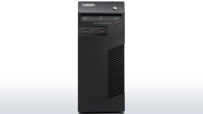
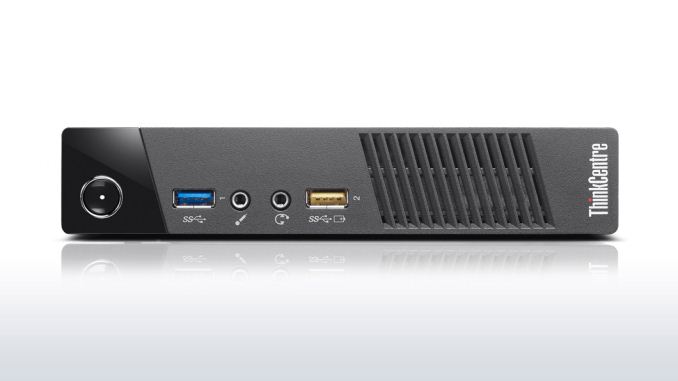
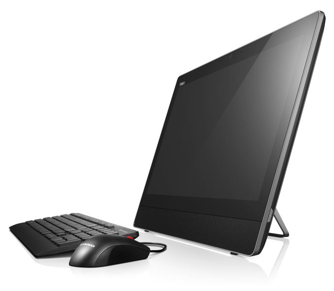
| 3:25p | Lenovo Announces Trio Of Business PCs
Lenovo has added three ThinkCentre desktop PCs to its stable of business devices this week. The three devices span the range of desktops, with the ThinkCentre E63z being an All-In-One, the ThinkCentre M53 being classified as a “tiny” desktop, and the ThinkCentre M79 offering the more traditional Small Form Factor (SFF) and Mini Tower models.
The typical office PC is likely a Mini Tower or SFF desktop, and the ThinkCentre M79 is an AMD A-Series APU equipped desktop offering optional Solid State Drive (SSD) or Solid State Hybrid Drive (SSHD) storage options in the SFF or Mini Tower configurations. Many businesses have moved to dual-displays for their desktop workers, and the M79 supports that out of the box, but also offers an optional second DisplayPort connector for those that want to move up to three displays. As a business PC, it also employs the Trusted Platform Module (TPM) version 1.2 for enhanced security feature support such as Bitlocker. It also includes version 3.0 of the Lenovo Intelligent Cooling Engine which controls the desktop acoustics and temperatures. Also of benefit to the business crowd, the M79 has a 15 month guaranteed hardware cycle to allow for an easier time managing system images. The ThinkCentre M79 is available now starting at $449.
The micro desktops from Lenovo have been around for a while, and the latest model to join the group is the ThinkCentre M53. Though larger than the NUC, the M53 is still extremely compact at 7.2” x 7.16” x 2.5” and can be vertically or horizontally arranged or can be mounted on the back of a monitor with VESA mounting holes on the underside of the device. The M53 shares accessories and power connectors with the other “tiny” computers from Lenovo which is always appreciated. The ThinkCentre M53 is available soon with a starting price of $439.
The final business aimed desktop is an all-in-one device called the ThinkCentre E63z. This unit features an integrated 19.5” display with optional touch, and an integrated camera and stereo speakers to allow for voice over IP and other collaboration software usage. Models equipped with the optional Core i3 CPU include an additional HDMI port, a card reader, and a Rapid Charge USB port for charging mobile devices. The E63z is available now starting at $479, with the Core i3 models available later this year. We do not have a full list of specifications for these devices at this time, but those should be available on the Lenovo site when they devices are made for sale. Source: | ||||
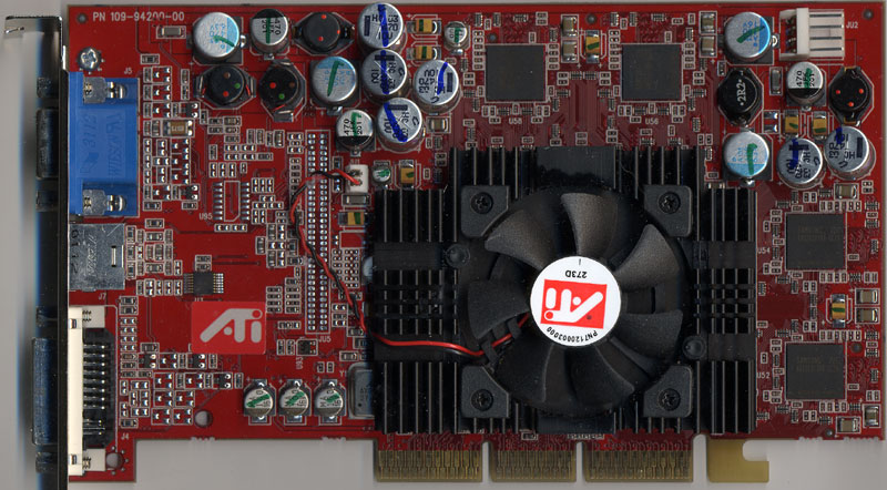
| 5:15p | AMD Celebrates 30 Years of Gaming and Graphics Innovation
AMD sent us word that tomorrow they will be hosting a Livecast celebrating 30 years of graphics and gaming innovation. Thirty years is a long time, and certainly we have a lot of readers that weren't even around when AMD had its beginnings. Except we're not really talking about the foundation of AMD; they had their start in 1969. It appears this is more a celebration of their graphics division, formerly ATI, which was founded in… August, 1985. AMD is apparently looking at a year-long celebration of the company formerly known as ATI, Radeon graphics, and gaming. While they're being a bit coy about the exact contents of the Livecast, we do know that there will be three game developers participating along with a live overclocking event. If we're lucky, maybe AMD even has a secret product announcement, but if so they haven't provided any details. And while we can now look forward to a year of celebrating AMD graphics and most likely a final end-of-the-year party come next August, why not start out with a brief look at where AMD/ATI started and where they are now?
I'm old enough that I may have been an owner of one of ATI's first products, as I began my By 1987, ATI began moving into the world of PC graphics with their "Wonder" brand of chips and cards, starting with 8-bit PC/XT-based board supporting monochrome or 4-color CGA. Over the next several years ATI would move to EGA (640x350 and provided an astounding 16 colors) and VGA (16-bit ISA and 256 colors). If you wanted a state-of-the-art video card like the ATI VGA Wonder in 1988, you were looking at $500 for the 256K model or $700 for the 512K edition. But all of this is really old stuff; where things start to become interesting is in the early 90s with the launch and growing popularity of Windows 3.0.
ATI's Mach 8 was their first true graphics processor from the company. It was able to offload 2D graphics functions from the CPU and render them independently, and at the time it was one of the few video cards that could do this. Sporting 512K-1MB of memory, it was still an ISA card (or it was available in MCA if you happened to own an IBM PS/2). Two years later the Mach 32 came out, the first 32-bit capable chip with support for ISA, EISA, MCA, VLB, and PCI slots. Mach 32 shipped with either 1MB or 2MB DRAM/VRAM and added high-color (15-bit/16-bit) and later True Color (the 24-bit color that we're still mostly using today) to the mix, along with a 64-bit memory interface. And two years after came the Mach 64, which brought support for up to 8MB of DRAM, VRAM, or the new SGRAM. Later variants of the Mach 64 also started including 3D capabilities (and were rebranded as Rage, see below), and we're still not even in the "modern" era of graphics chips yet!
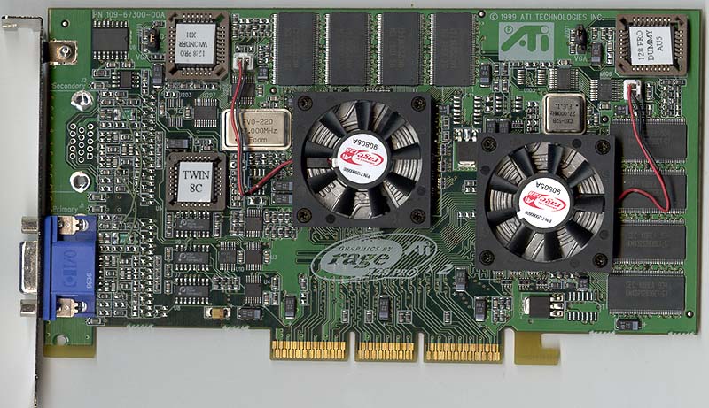
Next in line was the Rage series of graphics chips, and this was the first line of graphics chips built with 3D acceleration as one of the key features. We could talk about competing products from 3dfx, NVIDIA, Virge, S3, etc. here, but let's just stick with ATI. The Rage line appropriately began with the 3D Rage I in 1996, and it was mostly an enhancement of the Mach64 design with added on 3D support. The 3D Rage II was another Mach64 derived design, with up to twice the performance of the 3D Rage. The Rage II also found its way into some Macintosh systems, and while it was initially a PCI part, the Rage IIc later added AGP support. That part was followed by the Rage Pro, which is when graphics chips first started handling geometry processing (circa 1998 with DirectX 6.0 if you're keeping track), and you could get the Pro cards with up to 16MB of memory. There were also low-cost variations of the Rage Pro in the Rage LT, LT Pro, and XL models, and the Rage XL may hold the distinction of being one of the longest-used graphics chips in history, as I know even in 2005 or thereabouts there were many servers still shipping with that chip on the motherboard providing graphics output. In 1998 ATI released the Rage 128 with AGP 2X support (the enhanced Rage 128 Pro added AGP 4X support among other things a year later), and up to 32MB RAM. The Rage 128 Ultra even supported 64MB in its top configuration, but that wasn't the crowning achievement of the Rage series. No, the biggest achievement for Rage was with the Rage Fury MAXX, ATI's first GPU to support alternate frame rendering to provide up to twice the performance.
And last but not least we finally enter the modern era of ATI/AMD video cards with the Radeon line. Things start to get pretty dense in terms of releases at this point, so we'll mostly gloss over things and just hit the highlights. The first iteration Radeon brought support for DirectX 7 features, the biggest being hardware support for transform and lighting calculations – basically a way of offloading additional geometry calculations. The second generation Radeon chips (sold under the Radeon 8000 and lower number 9000 models) added DirectX 8 support, the first appearance of programmable pixel and vertex shaders in GPUs. Perhaps the best of the Radeon breed goes to the R300 line, with the Radeon 9600/9700/9800 series cards delivering DirectX 9.0 support and, more importantly, holding onto a clear performance lead over their chief competitor NVIDIA for nearly two solid years! It's a bit crazy to realize that we're now into our tenth (or eleventh, depending on how you want to count) generation of Radeon GPUs, and while the overall performance crown is often hotly debated, one thing is clear: games and graphics hardware wouldn't be where it is today without the input of AMD's graphics division! That's a great way to finish things off, and tomorrow I suspect AMD will have much more to say on the subject of the changing landscape of computer graphics over the past 30 years. It's been a wild ride, and when I think back to the early days of computer games and then look at modern titles, it's pretty amazing. It's also interesting to note that people often complain about spending $200 or $300 on a reasonably high performance GPU, when the reality is that the top performing video cards have often cost several hundred dollars – I remember buying an early 1MB True Color card for $200 back in the day, and that was nowhere near the top of the line offering. The amount of compute performance we can now buy for under $500 is awesome, and I can only imagine what the advances of another 30 years will bring us. So, congratulations to AMD on 30 years of graphics innovation, and here's to 30 more years!
| ||||
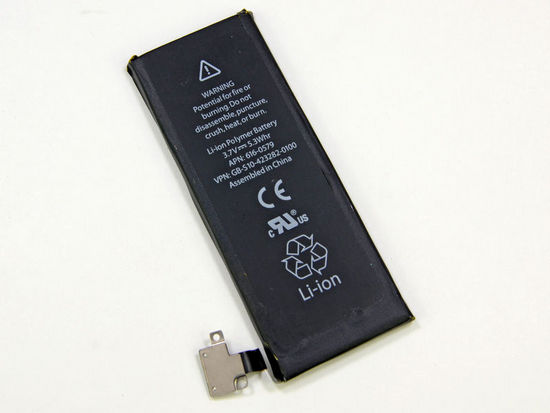
| 8:27p | Apple Begins iPhone 5 Battery Replacement Program for Certain Defective Devices
Today Apple has started a replacement program for certain iPhone 5 devices experiencing significantly reduced battery life. The company is stating that the affected devices were sold between the months of September 2012 and January 2013. Users with devices purchased within that timeframe who are experiencing issues are advised to check their serial number with Apple's new support page to see if they are eligible for a free battery replacement. Apple is also offering refunds to users with affected devices who paid for a battery replacement prior to the service program being launched. The replacement process for affected users will begin on August 22 in the United States and China, and on August 29 in the rest of the world. Apple recommends that users backup their iPhone to iTunes or iCloud and then wipe all user data prior to having their battery serviced. More information, as well as the service to check your device's serial number, can be found in the source link below. |


| << Previous Day |
2014/08/22 [Calendar] |
Next Day >> |