[Most Recent Entries] [Calendar View]
Monday, March 2nd, 2015
| Time | Event | ||||||||||||||||||||||||||||||||||||||||||||||||||||||||||||||||||||||||||||
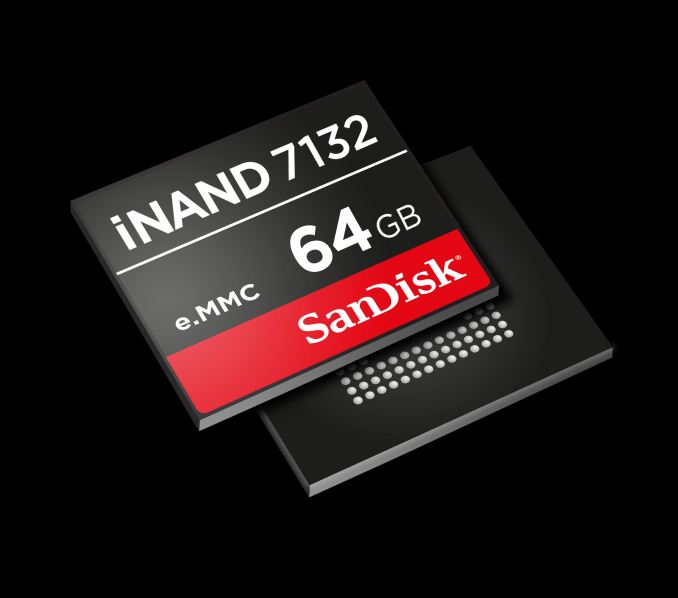
| 1:00a | SanDisk Announces iNAND 7132: SLC/TLC Hybrid eMMC
In general, storage performance has been an area that is only discussed when it becomes a bottleneck. There was very little focus on storage performance in general before devices like the original Nexus 7 started experiencing severe performance issues due to IO pauses. However, delivering high performance storage performance has generally limited storage SKUs to 32GB or less, as the cost of such storage is generally difficult to justify otherwise.
This is a problem that SanDisk hopes to solve with their new iNAND 7132, which uses a hybrid SLC/TLC architecture to deliver both high burst performance and cheaper storage for a given design. SanDisk claims that typical storage usage is extremely peaky in nature, even with seemingly contiguous data streams. In addition, relatively few cases can truly saturate modern eMMC on a smartphone even when using a TLC-based solution. By integrating an SLC cache into the eMMC package, it’s possible to achieve peak sequential reads of up to 280 MB/s, sequential writes of up to 125 MB/s, and up to 2800 and 3300 IOPS for random writes and reads, respectively. Based upon our discussions with SanDisk, it seems that the SLC cache is generally less than a gigabyte, but is usually enough to avoid situations where the SLC cache is filled and writes must go to the TLC storage. SanDisk has also implemented a great deal of error correction and extensively tested this storage solution, and claims that eMMC solution can last 10 years of 24/7 intense use without data loss. The iNAND 7132 eMMC 5.0 solution is currently available in 16, 32, and 64 GB variants, with a 128GB variant arriving mid-year. | ||||||||||||||||||||||||||||||||||||||||||||||||||||||||||||||||||||||||||||
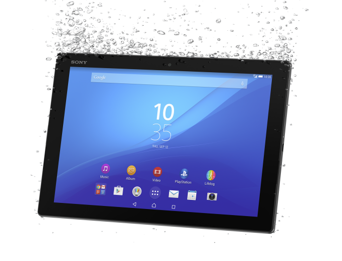
| 1:01a | Sony Announces the Xperia Z4 Tablet
Although much of the focus on Sony's work in the mobile space is on their smartphones, they have been a player in the tablet segment of the market for quite some time. In fact, Sony has been responsible for some of the more unique tablet designs, such as the Sony Tablet P which had two displays and folded much like a Nintendo DS. When focusing on what we traditionally think of as a tablet, one will see that the flagship device in Sony's lineup has always been their 10.1" tablet offering. These devices are usually named in the same "Xperia Z" format as Sony's flagship smartphones, and although the tablet released last year was the Xperia Z2 Tablet, the release of the Xperia Z3 Compact Tablet late last year means that this year's release moves ahead to Z4. The Xperia Z4 tablet is Sony's flagship tablet, and the first of 2015's high end Android tablets. To give an overview of the Z4 Tablet on paper, I've laid out its core specifications below.
Inside the Xperia Z4 Tablet we have Qualcomm's Snapdragon 810 SoC, which has four Cortex-A57 cores and four Cortex-A53 cores running at 2.0GHz and 1.6GHz respectively, along with Qualcomm's new Adreno 430 GPU. The internal battery remains the same capacity as the Z2 Tablet at 6000mAh (22.8Wh), but the tablet has been slimmed down to 6.1mm which puts it on par with Apple's iPad Air 2.
Moving to the outside of the tablet, we see that Sony has placed an 8MP camera on the rear, and a 5.1MP camera on the front. The front of the device is also home to the 10.1" 2560x1440 LCD display. Like many of Sony's recent devices, the Z4 Tablet is both dust and water resistant. It has an IP68 rating for which Sony specifies an immersion depth of up to 1.5 meters for up to thirty minutes, which goes a bit beyond the typical 1 meter for 30 minutes IP67 rating on many other mobile devices According to Sony, the Xperia Z4 Tablet will be launching globally in June. It will come in both WiFi and LTE variants, with pricing yet to be revealed. Source: Sony | ||||||||||||||||||||||||||||||||||||||||||||||||||||||||||||||||||||||||||||
| 2:00a | Imagination Announces PowerVR G6020 GPU & PowerVR Series 5 Video Encoder
With Mobile World Congress 2015 now in full swing, Imagination Technologies is taking to the show today to announce a couple of new additions to the PowerVR family of video products. First off is a new low-end GPU in the PowerVR Series6XE family, the G6020. The G6020 is aimed at entry-level mobile devices, embedded computers, and high-end wearables, and is intended to be Imagination’s new entry-level Series6XE part.
From a design perspective, the G6020 is aimed at very simple desktop workloads – the Android UI, wearable interfaces, etc. Imagination has essentially built the bare minimum GPU needed to drive a 720p60 display, taking out any hardware not necessary to that goal such as compute and quite a bit of geometry throughput. What remains is enough of a ROP backend (pixel co-processor) to drive 720p, and the FP16 shading resources to go with it. Meanwhile from a hardware perspective this is basically a significantly cut down 6XE part. G6020 drops to just a single 4 pipeline USC, versus the 8 pipeline USC found in the G6050, and 16 pipelines as found in a “complete” USC. The number of FP32 ALUs in each pipeline has also been reduced, going from the 6XE standard of 2 per pipeline to 1 for G6020, while the number of FP16 ALUs remains unchanged at 4. Along with scaling down the USCs, Imagination has also stripped down the G6020 in other ways, such as by taking out the compute data master.
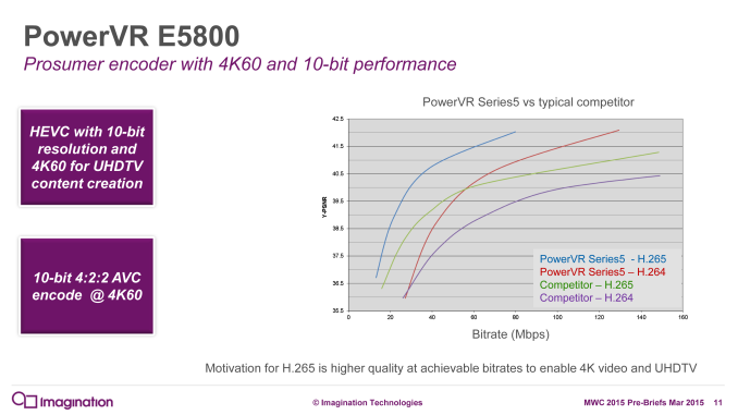
The end result of their efforts is designed to be an incredibly small and incredibly low power OpenGL ES 3.0 GPU for devices that fall in the cheap/small range. G6020 is only 2.2mm2 in size on 28nm, making it similar in size to ARM’s Cortex-A7 CPU cores (a likely pairing target). And power consumption is low enough that it should be able to just fit into high-end wearables. PowerVR Series 5 Video EncoderMeanwhile Imagination’s second PowerVR announcement of the day is the announcement of their new PowerVR Series 5 family of video encoders. This is Imagination’s entry into the HEVC (H.265) hardware encoder market, offering scalable designs for encoding H.264 and HEVC video.
In terms of designs Imagination will be offering 3 designs, the E5800, E5505, and E5300, targeted at progressively lower-end markets. The E5800 is the largest configuration and is aimed at the prosumer market, offering 4Kp60 encoding with 10-bit color and 4:2:2 chroma sampling (twice the sampling of standard 4:2:0 video). Below that is the E5505, the mainstream/premium mobile part with support for encoding up to 4Kp30, along with VP8 encoding and even MJPEG for certain legacy applications. Finally at the bottom of the list is the E5300, which is a small, low power encoder for 1080p30 applications (cameras/sensors/IoT and the like).
From a competitive standpoint, along with the expected synergy between the PowerVR encoders and PowerVR GPUs –support for directly handing off compressed memory, in particular – Imagination is also banking on being able to win a quality war with other mobile HEVC encoders. By Imagination’s estimates they can offer equivalent quality at just 70% of the bitrate, which would give them a significant advantage. The company says that this is a result of having a newer encoder that is better tuned than competing encoders, and one that implements more HEVC features (e.g. 10-bit color), allowing them to achieve better compression and the resulting reduction in bitrates.
While Imagination’s testing methodology and resulting numbers to get here are open to interpretation – PSNR is important, though not the end-all of encoder measurements – HEVC encoders are still a fledgling field. There is still ample opportunity to improve on HEVC encoders and reach the same kind of highly tuned status that H.264 encoders have evolved to. Wrapping things up, both new PowerVR products are now available for licensing. | ||||||||||||||||||||||||||||||||||||||||||||||||||||||||||||||||||||||||||||
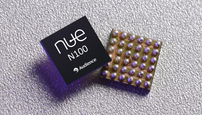
| 2:00a | Audience Announces NUE N100 Multisensor Processor
While Audience is traditionally focused on voice products, today they’re attempting to make their first moves into combined voice recognition and sensor hub products that leverage sensor fusion and neural networks. The NUE N100 is the first of this line of products, which is able to do keyword recognition and can keep the main CPU from waking until a command is received and registered. Audience focused on emphasizing how their solution eliminates the need for additional waiting once the initial wakeup occurs as it can cache the spoken command and feed it into a given system like Google voice actions. In addition, this solution is said to have reduced false wakeup rate, which means that there is far less power wasted on unintended activation. Audience’s solution can cache up to 5 key words, and can accurately distinguish between different people due to their use of neural network-based solutions, and can be programmed either by the end user or the OEM.
Outside of this VoiceQ system, Audience is also introducing MotionQ, which are contextual motion systems. In its current state, using various sensors present on a smartphone or tablet, the motion processing is able to determine whether the device is in a pocket, on a desk or in a person’s hand, whether the device is being held in a sitting, standing, walking or running position, and whether the device is in a car, train, bike, or many other contextual scenarios relying on the neural network algorithms as previously mentioned. The N100 also has OSP support, which means that OEMs can take the N100 and implement custom algorithms in addition to the work that Audience has already done. The N100 will be available for sampling in mid-2015, which means that devices shipping with this chip should appear around in 2016. | ||||||||||||||||||||||||||||||||||||||||||||||||||||||||||||||||||||||||||||
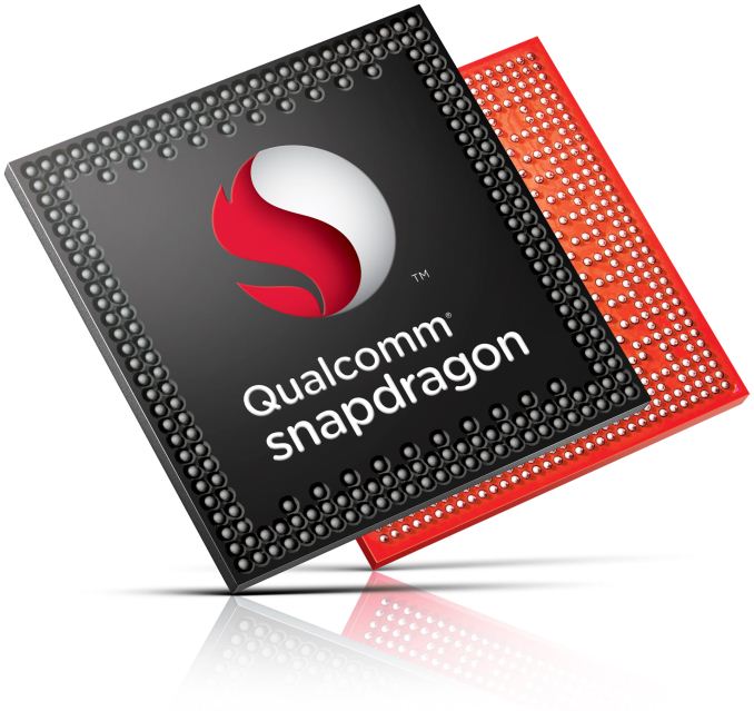
| 3:30a | Qualcomm Announces Snapdragon Sense ID Fingerprint Scanning
In addition to a new SoC, Qualcomm is announcing a new fingerprint sensing technology for Snapdragon-based devices. While most fingerprint sensors currently use high-resolution capacitive sensors, Qualcomm’s Snapdragon Sense ID uses ultrasonic sound waves in order to map the surface of the finger. This allows for greater resolution to recognize features such as pores and fingerprint ridges to improve security, along with reduced sensitivity to moisture and other contaminants. In addition, this technology can work through glass and sapphire cover lenses, along with metal and plastic casings. Snapdragon Sense ID will launch first on Snapdragon 810 and 425 devices, but will be compatible with all 400, 600, and 800 series Snapdragon SoCs, and will support the FIDO authentication standard. | ||||||||||||||||||||||||||||||||||||||||||||||||||||||||||||||||||||||||||||
| 3:30a | Qualcomm Announces Snapdragon 820 and Zeroth Platform
Today, Qualcomm is announcing the new Zeroth Platform, which is enabled by the Snapdragon 820 SoC. While Qualcomm is avoiding any real disclosure of the SoC at this point, we do know that the Snapdragon 820 will be built on a FinFET process, which could be either TSMC’s 16nm or Samsung’s 14nm process. In addition to all of the improvements that the move to a new process brings, Qualcomm is finally introducing their custom ARMv8 CPU core, named Kryo. Unfortunately, there are no real details here either, but given that there’s only one architecture named it’s likely that Qualcomm is moving away from big.LITTLE with the Snapdragon 820. The final detail regarding Snapdragon 820 is that it will begin sampling in the second half of 2015, which should mean that we can expect it to be in devices some time either at the end of 2015 or the beginning of 2016. Ultimately, the fact that Qualcomm has come up with a custom ARMv8 CPU architecture in such a short time continues to show just how quickly Qualcomm can respond to changing market conditions, something that we first saw with the Snapdragon 810. | ||||||||||||||||||||||||||||||||||||||||||||||||||||||||||||||||||||||||||||
| 4:10a | Qualcomm @ MWC 2015: Cat 11 LTE, Cat 6 Dual-Sim LTE, & LTE/Wi-Fi Link Aggregation
Not to be outdone by Qualcomm’s SoC group, Qualcomm’s communication groups are busy at MWC 2015 as well. Though Qualcomm Technologies and Qualcomm Atheros are not announcing any major new products at this moment, the two of them are on the show floor to demonstrate the status of their various LTE initiatives that we should see in upcoming and future products, in conjunction with infrastructure partner Ericsson. First and foremost, Qualcomm and Ericsson will be offering the first public demonstration of LTE category 11 hardware in action. LTE category 11 increases the download rate of LTE to 600Mbps through a combination of tri-band (3x20MHz) carrier aggregation and the use of QAM256 encoding, with the latter being the major addition of category 11. Due to the use of QAM256 and the higher SNR required to use it – not to mention 60MHz of spectrum – category 11 is being targeted at small scale deployments where cleaner signals and more spectrum is readily available, such as indoor deployments and carefully constructed outdoor environments.
Qualcomm is not currently announcing the modem being used in this demonstration. However we are likely looking at the successor to Qualcomm’s current X12 LTE modem (9x45), which tops out at category 10. Meanwhile Qualcomm will also be demonstrating the ability to use category LTE with dual SIMs. Qualcomm’s forthcoming hardware will support dual standby with dual receive. Finally, Qualcomm will also be demonstrating their current progress on implementing LTE/Wi-Fi call handoff and LTE/Wi-Fi link aggregation. With call handoff – or as Qualcomm likes to call it, Call Continuity – VoLTE calls can be seamlessly transferred between LTE and Wi-Fi, allowing phones to tap into Wi-Fi for call handling when possible, avoiding the greater network expense of using LTE. Meanwhile the first public demonstration of LTE/Wi-Fi link aggregation builds off of handoff to utilize both networks at once to take advantage of Wi-Fi speeds while allowing operators to better control a call via the normal LTE channel. Link aggregation essentially brings Wi-Fi access points under control of the LTE network itself – essentially limiting it to operator owned/controlled access points – and is being created as a solution to reliability concerns over using disparate, independent Wi-Fi networks. | ||||||||||||||||||||||||||||||||||||||||||||||||||||||||||||||||||||||||||||
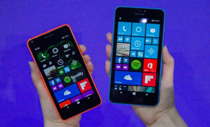
| 4:13a | Microsoft at MWC 2015: Lumia 640 and 640 XL Announced, 4K 120Hz Surface Hub Demoed
Mobile World Congress is in full swing today and Microsoft woke the press up early to discuss new features coming to their smartphone and tablet space. Top of the bill, presented by Stephen Elop, are the new Lumia 640 and Lumia 640XL devices. The regular 640, with it 5-inch HD display comes as the upgrade from the 630, whereas the 5.7-inch XL version sits as the move up from the large Lumia 1320.
Both devices will be available in 3G and LTE versions, with single and dual SIM in both of those depending on the market. The 640 uses a Snapdragon 400-series quad core processor at 1.2 GHz featuring Gorilla Glass 3, 1 GB of DRAM and 8 GB of storage. One might expect SD card support to come as standard, although a short hands on with the device failed to find one. The rear 8MP camera was described as a wide angle lens (although no numbers were given), with auto-HDR and dynamic LED flash. The battery weighs in at 2500 mAh also. Pricing for the 3G model starts at 139€ with the LTE version at 159€.
The 640 XL was described as ‘a slim 9mm’ with similar specifications to the smaller model but at 5.7 inches, namely a 1280x720 screen but the battery is pushed up to 3000 mAh. Internal specifications were not discussed, but the rear 13MP camera features Zeiss optics. Pricing starts at 189€ for the 3G model with LTE at 219€.
Both devices will ship with Windows 8.1 but will be upgraded to Windows 10, with Microsoft going all out to encourage Windows 10 across all of its future devices when available. The 640 and 640XL will also come with one year of Office 365, allowing installation on one PC and one other device as part of the deal. It also comes with 1TB of One Drive storage and 60 Skype World minutes.
An interesting element to the launch, especially with the ‘seemless feel’ push of Office across all different sizes of devices, was the Microsoft Universal Portable Keyboard. Barely bigger than a wallet, it is designed to fit into an office bag and be able to connect seamlessly via Bluetooth. No pricing or date was announced, but the focus was more on the office environment.
One demonstration that took me (Ian) by surprise was that of the Microsoft Surface Hub. This was an 84-inch display, normally the size used by large scale demonstrations, but this featured 4K resolution at 120 Hz as well as touch screen functionality. Naturally my thoughts drifted towards a TN type panel using MST, although taking the typical wide-angle test for TN panels was confusing as color consistency remained the same – it seems like they are using some kind of IPS display, which seems odd at 120 Hz.
The combination of 4K and 120 Hz and possibly IPS is mind boggling, which pointed me more towards an MST arrangement – either two panels or four. We managed to ask one of the product managers for the Surface Hub about this, but he was unable to give that information until launch. One of the demonstrations of the device featured a white-board scenario, as well as writing on office presentations. Anything written on the screen was recreated back to the controlling Surface tablet, and the tablet user could write as well, or what Microsoft calls ‘ink-back’. In a similar vein, ‘swipe-back’ to allow both users to change slides was demonstrated. The Surface Hub is linked to Windows 10, and we were told to expect more details at Windows 10 launch, along with another version at 55-inches but with 1080p resolution. Gallery: Microsoft at MWC 2015
      The final announcement of the presentation was for the Microsoft Build Conference, which will be on April 29th.
| ||||||||||||||||||||||||||||||||||||||||||||||||||||||||||||||||||||||||||||
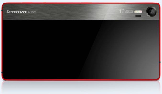
| 7:52a | Lenovo at MWC 2015: VIBE Shot SmartPhone/Camera Crossover Announced
As part of our booth tour at Lenovo during Mobile World Congress, on display was the recently announced Lenovo VIBE Shot and we managed to get some hands-on time. The VIBE Shot is described by Lenovo as a ‘2-in-1 camera smartphone’ attempting to bridge a gap between smartphones and point-and-click cameras. The device attempts this by placing buttons on the sides of the smartphone similar to how a point-and-click would do so, as well as having a full-frame 16:9 16MP low light sensor and a tri-color flash.
The 5-inch full HD device includes optical image stabilization as well as providing simple and pro modes with a button adjustment on the top. Simple mode is equivalent to the auto mode on most cameras, whereas the pro-mode offers manual adjustments such as exposure, white balance, focus mode, saturation and more. Hardware under the hood includes an eight-core Snapdragon 615 (A57/A57) at a 1.7 GHz peak on the fast cluster with 3GB DRAM and 32GB of internal storage.
Battery capacity comes in at 2900 mAh, with LTE Cat-4 and Android 5.0. The device will be offered in a dual Nano-SIM arrangement, weighs 145g and comes in at 7.3mm thin. Storage is expandable, with guaranteed support of up to 128GB via a microSD.
The phone felt pretty solid in hand, and the thinness is remarkable. What wasn't remarkable was the aluminium band on the back along the camera side, as it attracted fingerprints. The display unit had seen a lot of use, and it was quite hard to clean it.
The VIBE Shot will be available in red, white and grey, and come to Lenovo’s regular markets in June starting at $349. | ||||||||||||||||||||||||||||||||||||||||||||||||||||||||||||||||||||||||||||
| 9:00a | Intel at MWC 2015: SoFIA, Rockchip, Low Cost Integrated LTE, Atom Renaming and 14nm Cherry Trail
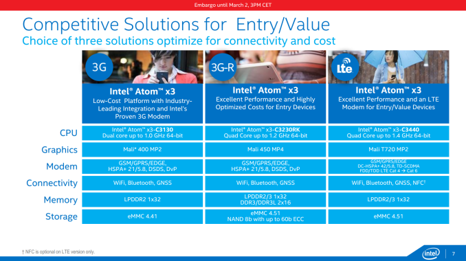
After day zero at Mobile World Congress already boasting some impressive releases, Intel tackles their platform on day one on several different fronts. As part of a pre-briefing, we were invited into the presentation where Intel discussed the current state of their mobile portfolio along with looking to the future. The pre-briefing was run by Aicha Evans, Corporate Vice President and General Manager of the Wireless Platform Research and Development Group, who you may remember was interviewed by Anand in a series of videos back in 2013. Ms. Evans' focus stems on the connectivity side of the equation, making sure that Intel’s portfolio develops into a strong base for future platforms. One of the big elements for Intel is the rebranding of their mobile Atom line of SoCs. Up until this point, all the SoCs were difficult to follow and very similar names such as Z3580 or Z3760. This is adjusted into three different segments as follows:
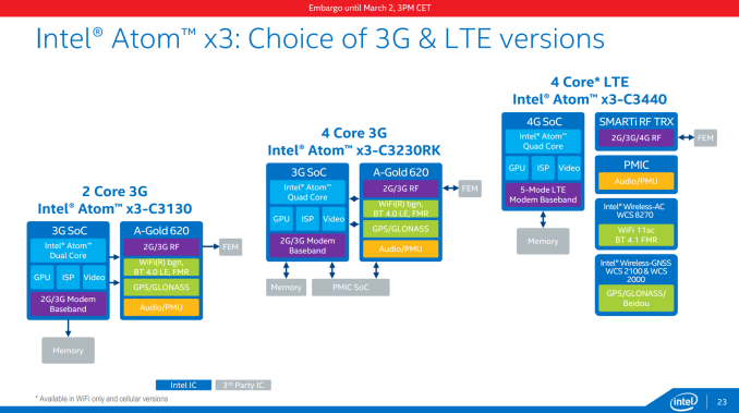
Similar to their personal computing processor line, the Intel Atom structure will take on x3/x5/x7 naming, similar to the i3/i5/i7 of the desktop and notebook space. This is not to be confused with Qualcomm’s modem naming scheme, or anything by BMW. The x3 sits at the bottom, and is comprised of Bay Trail based SoCs at the 28nm node all previously part of the SoFIA program aimed at emerging markets. There will be three x3 parts – a dual core x3, a quad core x3 from the Rockchip agreement, and a final quad core x3 with an integrated LTE modem.
This set raises some interesting points to discuss. Firstly is the use of 28nm is the same node as previous Intel Atoms, and thus should be derived from a TSMC source. It is also poignant to note that for these SoCs Intel is using a Mali GPU rather than the Gen 8 graphics and their own IP. This is due to the SoFIA program being aimed at bringing costs down and functionality into the low price points in a competitive time-to-market.
The Rockchip model, indicated by the ‘RK’ at the end of the name of the SoC, comes from the partnership with Rockchip we reported on back in May 2014. At the time Intel discussed the roadmap for producing a quad core SoC with 3G for the China market in the middle of 2015, which this provides.
The final part of the x3 arrangement revolves combining a 5-mode LTE modem on the same die. Intel is going to support 14 LTE bands on a single SoC with PMIC, WiFi and geolocation technologies (GPS, GLONASS, BeiDou).
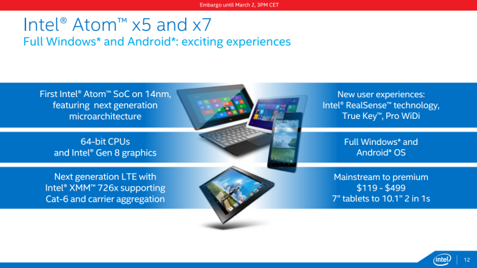
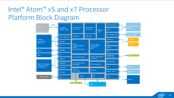
The Atom x5 and x7 SoCs represent the next step up, implementing Intel’s 14nm process and bringing Cherry Trail to market. The x5 and x7 SoCs are aimed primarily at tablets, but can find their way into sub 10.1 inch tablets as well, providing an interesting counterbalance to the high price premium of Intel Core-M 4.5W products based on Broadwell-Y. While the x3 line will focus first on Android moving into Windows, x5 and x7 is designed to be targeting both, particularly with the bundled Gen 8 graphics and LTE with XMM276x supporting Cat-6 and carrier aggregation.
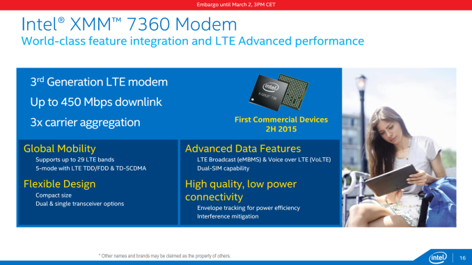
Not a lot of detail was provided about x5 and x7, suggesting that they are aimed more at late 1H/2H 2015 down the line. This coincides with the next generation of Intel’s XMM 7360 modem, featuring up to 450 Mbps downlink and support for up to 29 LTE bands.
One interesting element in the x5/x7 scenario was the bundled platform block diagram provided by Intel, showing clearly the two dual-core Airmont CPUs each with 1MB of L2 cache, Gen 8 graphics, separate security processors and ISP, as well as USB 3.0 support.
Finally, Intel addressed the obvious lack of a high-end mobile SoC that fits into the performance smartphone category. Intel is still working on development of such a SoC in the form of Braxton and we'll have more news on this piece in the future. We are lining up a chance to interview Ms. Evans about Intel’s Atom lineup later this week at MWC, so stay tuned for that. | ||||||||||||||||||||||||||||||||||||||||||||||||||||||||||||||||||||||||||||
| 5:00p | Broadcom at MWC 2015: BCM4359 and BCM43455 Wifi Combo Chips Announced
Today Broadcom took the lead by announcing two new Wifi combo chip solutions meant for the smartphone and tablet market. The BCM4359 is a high-end 2x2 MIMO solution for high-performance smartphones, while the BCM43455 is an updated 1x1 MIMO 802.11ac for mass market phones. Taking a closer look at the BCM4359, we see several innovative new features, the most characterizing one being the inclusion for the first time of Real Simultaneous Dual Band (RSDB). RSDB enables the chip to connect to both 2.4GHz and 5GHz bands simultaneously. This is achieved by doubling up on the baseband processors on the combo chip. Broadcom uses ARM Cortex R4 as the processing units of the IC, and the 4359 uses two of them. What this enables is a sort of "full duplex" on the two frequency bands instead of having the baseband having to switch between each in an interleaving manner. The PHY bandwidth has been upped to 867 Mbps in the two-stream MIMO mode. In the demo that Broadcom showed us, we had two test devices and a TV as the showcase setup. One device running the BCM4356 was streaming a video to the secondary device which employed the BCM4359 via the 2.4GHz band, who in turn would then stream via Wifi Display on 5GHz to the TV. As a comparison demo, we had the same setup next to it, but with both streaming devices equiped with only a BCM4356 solution. While the BCM4359 setup managed to achieve enough bandwidth to receive and forward the stream to the TV in full 1080p, the other side with the BCM4356 would only be fluid if the quality was reduced to 480p. Another advantage of RSDB is that it enables the chip to scan for networks on both bands simultaneously, accelerating the time needed to show available Wifi networks, effectively giving a 2x speed improvement.
The BCM43455 is also a new member of the Broadcom family and serves as a solution for the mass market, meaning a cheaper price-point. It is a 1x1 HT80 802.11ac 2.4 and 5GHz solution, enabling up to a 433Mbps PHY rate at 80MHz channel bandwidth. The chip is able to reduce the BoM by 50%, although Broadcom didn't specify to what this was compared with. One key aspect of these new Wifi generation chips is that SDIO has been retired (but still available as a seconary option) as the connection interface to the SoC and instead replaced by PCIe. The BCM4358 was the first such chip to take advantage of this switch, which was employed on for example the Galaxy Note 4. The PCIe interface not only provides higher bandwidths which are beyond what SDIO is capable of, but also enables crucial power advantages such as low power states on the bus and bonuses such as Direct Memory Access (DMA) for the Wifi chipset. Both the BCM4359 and BCM43455 are sampling now and will be available in devices later in the year. | ||||||||||||||||||||||||||||||||||||||||||||||||||||||||||||||||||||||||||||
| 10:45p | AMD Lays Out Future of Mantle: Changing Direction In Face of DX12 and glNext
Much has been made over the advent of low-level graphics APIs over the last year, with APIs based on this concept having sprouted up on a number of platforms in a very short period of time. For game developers this has changed the API landscape dramatically in the last couple of years, and it’s no surprise that as a result API news has been centered on the annual Game Developers Conference. With the 2015 conference taking place this week, we’re going to hear a lot more about it in the run-up to the release of DirectX 12 and other APIs. Kicking things off this week is AMD, who is going first with an update on Mantle, their in-house low-level API. The first announced of the low-level APIs and so far limited to AMD’s GCN’s architecture, there has been quite a bit of pondering over the future of the API in light of the more recent developments of DirectX 12 and glNext. AMD in turn is seeking to answer these questions first, before Microsoft and Khronos take the stage later this week for their own announcements. In a news post on AMD’s gaming website, AMD has announced that due to the progress on DX12 and glNext, the company is changing direction on the API. The API will be sticking around, but AMD’s earlier plans have partially changed. As originally planned, AMD is transitioning Mantle application development from a closed beta to a (quasi) released product – via the release of a programming guide and API reference this month – however AMD’s broader plans to also release a Mantle SDK to allow full access, particularly allowing iit to be implemented on other hardware, has been shelved. In place of that AMD is refocusing Mantle on being a “graphics innovation platform” to develop new technologies. As far as “Mantle 1.0” is concerned, AMD is acknowledging at this point that Mantle’s greatest benefits – reduced CPU usage due to low-level command buffer submission – is something that DX12 and glNext can do just as well, negating the need for Mantle in this context. For AMD this is still something of a win because it has led to Microsoft and Khronos implementing the core ideas of Mantle in the first place, but it also means that Mantle would be relegated to a third wheel. As a result AMD is shifting focus, and advising developers looking to tap Mantle for its draw call benefits (and other features also found in DX12/glNext) to just use those forthcoming APIs instead.
Mantle’s new focus in turn is going to be a testbed for future graphics API development. Along with releasing the specifications for “Mantle 1.0”, AMD will essentially keep the closed beta program open for the continued development of Mantle, building it in conjunction with a limited number of partners in a fashion similar to how Mantle has been developed so far. Thie biggest change here is that any plans to make Mantle open have been put on hold for the moment with the cancelation of the Mantle SDK. With Mantle going back into development and made redundant by DX12/glNext, AMD has canned what was from the start the hardest to develop/least likely to occur API feature, keeping it proprietary (at least for now) for future development. Which is not to say that AMD has given up on their “open” ideals entirely though, as the company is promising to deliver more information on their long-term plans for the API on the 5th, including their future plans for openness.
As for what happens from here, we will have to see what AMD announces later this week. AMD’s announcement is essentially in two parts: today’s disclosure on the status of Mantle, and a further announcement on the 5th. It’s quite likely that AMD already has their future Mantle features in mind, and will want to discuss those after the DX12 and glNext disclosures. Finally, from a consumer perspective Mantle won’t be going anywhere. Mantle remains in AMD’s drivers and Mantle applications continue to work, and for that matter there are still more Mantle enabled games to come (pretty much anything Frostbite, for a start). How many more games beyond 2015 though – basically anything post-DX12 – remains to be seen, as developers capable of targeting Mantle will almost certainly want to target DX12 as well as soon as it’s ready. Update 03/03: To add some further context to AMD's announcement, we have the announcement of Vulkan (aka glNext). In short Mantle is being used as a building block for Vulkan, making Vulkan a derivative of Mantle. So although Mantle proper goes back under wraps at AMD, "Mantle 1.0" continues on in an evolved form as Vulkan. | ||||||||||||||||||||||||||||||||||||||||||||||||||||||||||||||||||||||||||||


| << Previous Day |
2015/03/02 [Calendar] |
Next Day >> |