[Most Recent Entries] [Calendar View]
Wednesday, August 12th, 2015
- Zotac’s Hey Good Lookin’: Adam Abadir of Austin, TX
- Corsair’s The Accelerator: David Baron of Gilbert, AZ.
| Time | Event |
| 8:00a | Build-A-Rig Round 1: The Winners
As our final update to what has been a very successful first round for our Build-A-Rig project, last week we held the drawing to determine the winners. Each of our winners is taking home a $1500 gaming system, designed by Zotac and Corsair respectively. So without further ado:
Congratulations to our two winners, and the first winners for the Build-A-Rig project. And be sure to check back later this month when we kick off Build-A-Rig round 2, where we will be putting together and giving away a pair of small form factor systems. |
| 8:00a | Advatronix Nimbus 400 File Server Review Small businesses and power users often need the flexibility offered by a file server when compared to a dedicated NAS. This is where storage servers based on Microsoft's Windows Server offerings and systems based on various Linux and BSD distributions come into play. These servers can be bought as an appliance or assembled in a do-it-yourself (DIY) fashion. Today, we will be looking at a system based on the former approach - the Advatronix Nimbus 400. |
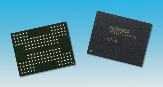
| 8:01a | Toshiba Brings Through-Silicon Vias to NAND Flash
At Flash Memory Summit this week, Toshiba is showing off a NAND flash device packaged using through-silicon vias rather than traditional wire-bonded connections. The NAND flash currently on the market is typically produced in the form of a die with a capacity like 128Gb (16GB). The popular SSD form factors don't have enough surface area to fit dozens of those chips, and SSD controllers don't have the pin count to connect to that many independently, so several chips are stacked in a single postage-stamp sized package. The traditional way of connecting the individual dies in a stack is to use the same technique as for a single-die package: bonding a thin gold wire between the edge of the die and the package substrate or external pins. The downsides are that it requires a lot of wires and the edges of the dies in the stack need to be exposed somehow, either by staggering them or by putting a spacer between each layer.
An alternative packaging method is to design the dies to participate in the stacking, by including electrical conductors that penetrate the entire thickness of the silicon die so that they can make contact with the dies above and below it in the stack, essentially tunneling right through each die. These through-silicon vias (TSVs) can then form a shared bus to carry signals from any of the dies in the stack out to the last die, which is the only one with the external connections.
Chip stacking using TSVs requires the dies to be aligned and stacked without spacers, which makes the whole stack a bit more compact. Since TSVs can be placed anywhere on the chip rather than just at the edge, it's easy to implement a wide data bus and communication within the stack can be very fast or low-power due to the short distances involved. These advantages have been very attractive for packaging DRAM, most notably in the form of the HBM stacks used by AMD's R9 Fury and R9 Nano video cards. Toshiba's demonstration is a 16-high stack of 128Gb dies in a BGA-152 package measuring 14mm by 18mm and 1.9mm thick, and an 8-high stack that's 1.35mm thick. Those numbers are all typical even for wire-bonded stacks. The speed (1Gb/s) and operating voltages (1.2V for I/O and 1.8V core) are what we would expect from a next-generation NAND interface, but the claimed 50% power reduction is a very nice improvement for a change that leaves the flash memory cells themselves unmodified. Toshiba hasn't said whether the dies being stacked are their current 15nm planar NAND or their forthcoming 3D NAND, nor have they said when modules using TSVs will be hitting the market. The most compelling applications would be to use TSVs to stack flash atop a controller chip in an eMMC product or atop an SoC, but the power savings would be appreciated almost everywhere. If the use of TSVs allows economically stacking more than 16 dies, it could enable a dramatic increase in the density of SSDs. |
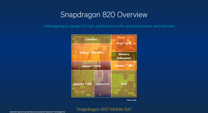
| 9:35a | Qualcomm Details the Adreno 530 GPU and ISP inside the Snapdragon 820
Snapdragon 820 is still a mystery as far as official information from Qualcomm goes. However, today Qualcomm has given a bit of insight into their upcoming SoC. While there's still no information about the CPU portion featuring Qualcomm's custom 64-bit cores known as 'Kryo', there are some details about the Adreno 510 and 530 GPUs, as well as Qualcomm's Spectra image signal processor.
Because Adreno 530 is their new flagship GPU, Qualcomm's press release focuses more on the 530 than the 510. The performance figures released by Qualcomm describe Adreno 530 as being 40% faster than Adreno 430 on average, while also consuming 40% less power. This result is described as an average of "the top graphics benchmarks", and while it's still generally a good idea to take vendor provided numbers with a grain of salt, if the power and performance gains over Adreno 430 are anywhere in the ballpark of Qualcomm's 40% figure then Adreno 530 should end up being quite impressive.
On the API side, Adreno 500 series GPUs will support OpenGL ES 3.1 + AEP (Android Extension Pack), Renderscript, Vulkan, and OpenCL 2.0. With OpenCL 2.0 comes support for Shared Virtual Memory (SVP), which allows an OpenCL host program and a device's kernel to share a virtual address space so access to data structures like lists and trees can be easily shared between the host and GPU. Adreno 530 has varying improvements to GPGPU performance when compared to Adreno 430, but Qualcomm's slides show video processing as demonstrating the greatest improvement with a 2.5x increase in compute performance. This is also the area where efficiency gains for generational improvements typically happen, so we expect fixed-function codec support although this information is not yet provided. As for the ISP, it's still the case that mobile image signal processors are black boxes. Qualcomm is stating that their Spectra ISP in Snapdragon 820 will be able to support 3 simultaneous cameras at up to 25MP and at 30fps with no shutter lag. The Spectra ISP will also use MIPI's higher bandwidth C-PHY serial interface, which supports the enhanced camera support. As well as this, new developer and user-facing features include support and APIs for depth maps and using dual cameras to perform refocusing or other visual effects - because Qualcomm is just the SoC manufacturer, it is up to the smartphone OEMs to implement dual-camera/depth-maps as a feature as well. According to Qualcomm, Snapdragon 820 will start showing up in devices during the first half of 2016. Hopefully between now and then there's more information from Qualcomm about the other aspects of their new SoC, including their Kryo custom CPU core. In Q1 we will be at Mobile World Congress, so we may see more information at that time. |


| << Previous Day |
2015/08/12 [Calendar] |
Next Day >> |