[Most Recent Entries] [Calendar View]
Thursday, February 11th, 2016
| Time | Event | |||||||||||||||||||||||||||||||||
| 8:00a | The Lenovo Ideapad Y700 Laptop Review The PC gaming market has been pretty strong market over the last couple of years, and recent developments have pushed the boundaries again. With launches of virtual reality headsets, we’ve seen even notebook manufacturers getting prepared to drive these new devices, but it takes a lot of compute to do it. Manufacturers going after sales of gaming notebooks are going to be able to eke out better margins too, so it’s an area many of them focus on. But the typical gaming notebook is going to be quite expensive. A powerful mobile GPU, nice display, and good processor, are all going to add to the bill of materials. For those that want to get into the market for a gaming notebook, sometimes you don’t want to break the bank. | |||||||||||||||||||||||||||||||||
| 9:00a | EVGA Begins Selling "VR Edition" GeForce GTX Video Cards for VR Gaming Rigs
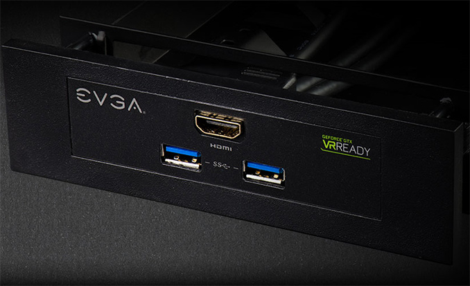
EVGA this week began to sell their GeForce GTX 980 Ti VR Edition video cards, a new lineup tailored for those who plan to use a virtual reality headset. The graphics boards are equipped with an internal HDMI port and a special adapter for 5.25-inch bay that simplifies plugging VR headsets to PCs. The family of EVGA’s VR Edition graphics cards currently includes two models, both of which are modifications of EVGA's existing GTX 980 Ti card designs. The first VR Edition card is the EVGA GeForce GTX 980 Ti VR Edition Gaming ACX 2.0+ (06G-P4-3996), which uses the company’s own ACX 2.0+ cooler featuring 8-mm copper heatpipes, aluminum radiators, two fans and a memory/MOSFET cooling plate, while the second is the EVGA GeForce GTX 980 Ti VR Edition Gaming (06G-P4-3998), which uses NVIDIA’s reference cooler for high-end boards. As these are GTX 980 Ti cards, both cards are based on the GM200 GPU with 2816 stream processors, 176 texture units, 96 ROPs as well as a 384-bit memory bus. The GPUs are clocked at 1000 MHz/1076 MHz (base/boost), whereas the attaced 6 GB of GDDR5 memory is clocked at 7 Gbps.
A brief examination of the pictures provided on EVGA's website indicates that both VR Edition graphics cards are using PCBs that resemble NVIDIA’s reference designs for the GeForce GTX 980 Ti/Titan X (8pin + 6pin power inputs), but they feature an important addition. The adapters have an internal HDMI 2.0 port that connects to a special adapter for 5.25-inch bay that has an HDMI output as well as two USB 3.0 connectors. The adapter is designed to connect the Oculus Rift, the HTC Vive or any other VR headset to a PC without using ports on the backside of the computer, which makes the process considerably more comfortable.
EVGA's product literature indicates that they're primarily focused on first-time buyers - those who will be building or upgrading systems ahead of the spring VR headset launches - as these headsets will be launching some time before any 16nm high-end GPUs. That said, I wouldn't be surprised if the VR Edition cards also proved popular with gamers who already have a PC powered by the GeForce GTX 980 Ti and are looking forward to build a multi-GPU system to play VR games, as VR SLI scaling is looking optimisitc thanks to the ability to forgo AFR and assign a GPU to each eye. From a design perspective, routing HDMI port to the backside of the card should be relatively easy. EVGA hasn't released any board shots, but they likely only had to slightly modify voltage regulating module of their GeForce GTX 980 Ti boards without any significant changes to its design. Consequently I wouldn't be surrprised if other makers of video cards do something similar later on - the idea seems rather obvious in hindsight - though for the moment EVGA is the first and only game in town. Perhaps, if VR gaming takes off in the next year or two, AMD and NVIDIA could add internal graphics ports to their reference designs.
Both EVGA GeForce GTX 980 Ti VR Edition graphics cards are available now for $699, which comes at around a $70 premium over their normal reference-clocked GeForce GTX 980 Ti boards (usually $620 - $630). As it appears, VR gamers will have to pay a extra for the VR adapter for 5.25” bays. However, given the additional comfort, it may well worth the investment, especially for those who plan on frequently plugging and unplugging VR headsets (or for that matter even tradtional HDMI displays). | |||||||||||||||||||||||||||||||||
| 9:18a | Qualcomm Announces Snapdragon 625, 425 & 435 Mid- and Low-End SoCs
Today Qualcomm announces three new SoCs in the mid- and low-end Snapdragon lineup. At the lowest end we find the Snapdragon 425 offering a very frugal CPU configuration consisting of 4x Cortex A53's clocked in at 1.4GHz. The chipset is aimed at replacing the Snapdragon 410 and 412 and improves on them with an upgrade on the modem block as well as media decoder and encoder capabilities, now enabling 1080p HEVC decode and encode. The Snapdragon 435 replaces the Snapdragon 430 which was only announced just a few months ago and also sees an improvement in the modem block used as we see it now going from UE Category 4 to UE Category 7. On the CPU side we see a 200MHz boost in the frequency of the faster of the two quad-core A53 clusters, now reaching 1.4GHz. In both the Snapdragon 425 and 435 we don't see a change in the GPU but it's possible clocks have changed; Unfortunately details on the matter are still sparse. Both the Snapdragon 425 and 435 are manufactured on a "28nm LP" process but sadly it wasn't specified which foundry is manufacturing them.
Most importantly comes the announcement of the Snapdragon 625. This is the successor to the Snapdragon 617 which along with the 615 has seen quite a lot of success in mid-range and budget smartphones. The CPUs remain two quad-core clusters of Cortex A53's but now the performance cluster is clocked at up to 2GHz representing a large increase to the 1.5GHz SoCs which the 625 is replacing. The GPU has also been upgraded from an Adreno 405 to a newer generation Adreno 506. The modem again has seen a slight upgrade from an X8 to an X9 block, allowing for an increase in the uplink performance if the network supports it. The biggest surprise out of today's announcements is the fact that the Snapdragon 625 is manufactured on Samsung's/GlobalFoundry's 14nm LPP process. Qualcomm thus is the first vendor to announce a non-high-end SoC to use a new FinFET manufacturing process which is quite astonishing as I hadn't expected vendors be able to do the migration so early on in the technology's lifetime, which may be a positive indicator that we might be seeing FinFET adopted across the mid-range earlier than expected. The new SoC should be sampling to vendors in mid-2016 with availability in commercial devices in the second half of 2016. | |||||||||||||||||||||||||||||||||
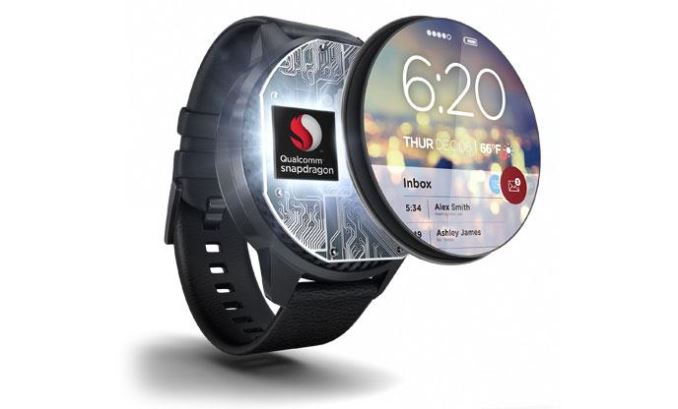
| 10:19a | Qualcomm Announces Snapdragon Wear 2100 IoT SoC
Along with today's announcements of the Snapdragon 425, 435 and 625, we also see the reveal of a new wearables-oriented SoC: the Snapdragon Wear 2100. In the past we've seen vendors use low-end smartphone SoCs such as the Snapdragon 400 (Motorola Moto 360 2nd gen). In fact, to date only Samsung (Exynos 3250) and Apple (S1) were able to employ chipsets that were specifically designed for wearables. This was rather unfortunate for other wearable vendors as devices such as smartwatches require much higher efficiency and lower power than what "off-the-shelf" SoCs were able to offer. Qualcomm sees to fix this by introducing a new lineup of chips called Snapdragon Wear that are designed with wearables in mind. The Snapdragon Wear 2100 is a quad-core Cortex A7 running at up to 800MHz or 1.2GHz (Qualcomm at various points states both) with an Adreno 304 GPU and 400MHz LPDDR3. The choice of using a Cortex A7 is warranted by the fact that Cortex A53s are too power hungry for wearables and that it's likely too early to see Cortex A35 based SoCs as ARM announced the core only a couple of months ago. A big advantage that Qualcomm has with the Wear 2100 is that it's able to offer an integrated X5 modem for basic cellular connectivity (Supporting all current standards). With the Wear 2100 Qualcomm is now able to offer a fitting SoC for wearable devices and it's very likely that consumers will see direct benefits such as improved battery life. Qualcomm hasn't specified any availability for the SoC but discloses that there are multiple devices in development using the processor. | |||||||||||||||||||||||||||||||||


| << Previous Day |
2016/02/11 [Calendar] |
Next Day >> |