[Most Recent Entries] [Calendar View]
Monday, February 22nd, 2016
| Time | Event | ||||||||||||||||||||||||||||||||||||||||||||||||||||||||||||||
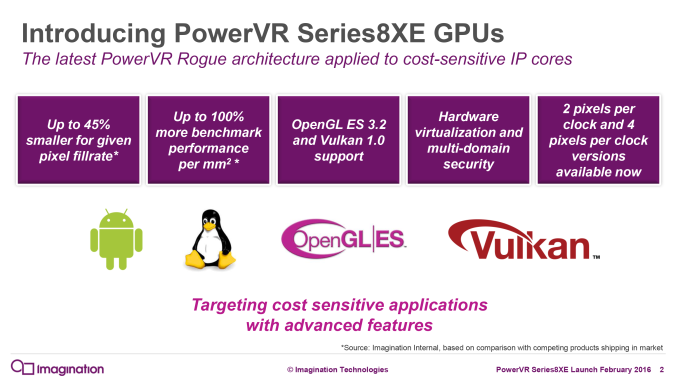
| 2:00a | Imagination Announces PowerVR Series8XE Family - Entry-Level GPUs Get Smaller
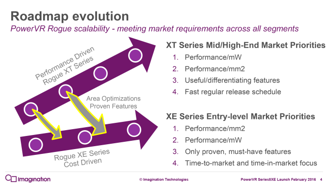
With Mobile World Congress 2016 now in full swing, we’ll see a slew of announcements this week. Among the crowd is Imagination Technologies, who is using the show as a backdrop to discuss their latest generation of GPU technologies. To that end, today the company is announcing the latest iteration of their Rogue architecture for the entry-level SoC GPU market, PowerVR Series8XE. Throughout the lifetime of the Rogue architecture, Imagination has offered two families of designs: the XT family for high performance devices, and the XE family for cost-sensitive entry-level devices. As this is the SoC space both families are focused on power efficiency, but whereas the XT family focuses on a higher overall class of features and performance, the XE family focuses on minimizing overall die size and including a smaller, core set of features. And though both get similar Series branding (e.g. Series7), it’s perhaps more accurate to say both are separate takes on the Rogue architecture, sharing technologies where it makes sense but also being more differentiated than simply their performance targets.
In any case, in a break from tradition, for their newest integration of the Rogue architecture Imagination is not announcing both the XT and XE parts at the same time this year. Rather it’s solely the entry-level Series8XE that’s getting announced at this time, making it Imagination’s sole MWC 2016 GPU announcement. With Series8XE the underlying Rogue architecture has not significantly changed from previous iterations, however Imagination has continued to optimize it for the low cost and low power markets this GPU family is targeted at. Like Series7XE, this ranges from high-end wearables and IoT devices up to midrange phones and tablets.
From a technical perspective, compared to the last-generation Series7XE, Series8XE gains a couple of notable features. 8XE is OpenGL ES 3.2 capable (versus 3.1 for the base 7XE configuration), updating the GPU to support the latest feature sets required for ES 3.2 while also providing those features for Vulkan. And although Imagination doesn’t explicitly state it, that this isn’t listed as a separate, optional feature implies that tessellation and ASTC are now base features for 8XE. Meanwhile support for OmniShield, the company’s hardware security zone technology has also been added to the base feature set, and from the way Imagination has talked about it, it sounds like they expect OmniShield to be a greater differentiating feature this generation.
As for optional features, 10-bit YUV is still offered as an option in the design, primarily for unencumbered HEVC Main10 playback. Also optional for 8XE is the latest generation of Imagination’s PowerVR image compression technology, PVRIC3. Imagination isn’t detailing every last change for PVRIC3, but they are noting that this generation of the technology has full integration with their video decoder and texture decoder, allowing for resources to be passed from the video decoder into the display buffer or into the texture decoders in a compressed format, whose smaller size saves power by virtue of lower memory bandwidth needs and cache pressure. But by far the biggest focus for Imagination for 8XE appears to be on the overall footprint of the GPU designs, with the company continuing to push down the size of their GPUs. Imagination tells us that their 8XE designs are around 25% smaller than 7XE designs for the same pixel fillrate, and smaller still than competing designs (which these days we’d assume to be ARM Mali). Ultimately the push here is to bring down the manufacturing costs of their GPUs, as every square millimeter saved further reduces the total SoC size and cost in what is a very competitive market for entry-level SoCs.
To get there, Imagination is basing the 8XE designs around maximizing pixel fillrate, while also making fillrate the primary performance metric for their designs. Imagination tells us that they believe that pixel fillrate is the biggest resource need for entry-level devices and other low-end GPU consumers right now, as simple tasks such as web browsing and casual games aren’t making heavy use of pixel shader operations. And although the company isn’t talking about specific details here – preferring to keep their secret sauce secret - it’s implied that the company has changed the overall balance between pixel shading resources, compute resources, and pixel fillrate resources in order to hit their performance goals while still producing a more compact design than 7XE. At this point the company tells us that
Digging a bit deeper, 8XE’s USC and pixel co-processor are actually very similar to 7XE. A single USC pipeline still contains 4 FP16 ALUs, 2 FP32 ALUs, and a SFU ALU. Meanwhile the pixel co-processor still produces either 2 or 4 pixels per clock, depending on the specific implementation. In which case 8XE’s theoretical per-clock performance is very similar to 7XE’s, and that any rebalancing done by Imagination likely took place in the various frontend data masters and thread scheduling hardware that feed the GPU. Moving on, for today’s announcement of Series8XE, Imagination is also announcing the first two 8XE GPU designs, the GE8300 and GE8200. These designs are the successors to the 7XE-based GE7800 and GE7400 respectively, with the GE8300 implementing a whole USC (16 pipelines), while the GE8200 is essentially half of a GE8300, implementing half of a USC (8 pipelines). Similarly, pixel throughput per clock is unchanged from their predecessors, with GE8200 offering 2 pixels per clock while GE8300 offers 4 pixels per clock. Between the two GE8200 is primarily targeted at the true entry-level markets – along with the high-end wearables market – while GE8300 is for higher performance mobile devices and 4K TVs.
Wrapping things up, although Imagination does not announce when to expect SoCs utilizing their designs to hit the consumer market, they are announcing that they’ve already struck licensing deals for Series8XE for TVs, wearables, and automotive designs. All of which are no doubt welcome developments for the company in what has been a highly competitive market for entry-level GPUs. | ||||||||||||||||||||||||||||||||||||||||||||||||||||||||||||||
| 2:08a | MWC 2016: Sony Press Conference Live Blog We're here at Sony's booth for their annual MWC press conference. There are plenty of press here, and not a lot of space, but we're looking forward to the announcements! | ||||||||||||||||||||||||||||||||||||||||||||||||||||||||||||||
| 8:16a | MWC 2016: Gionee Press Conference S8 Launch Live Blog I'm sat here at the Gionee press event! All the signs say S8 launch, so I guess it's an S8 launch? | ||||||||||||||||||||||||||||||||||||||||||||||||||||||||||||||
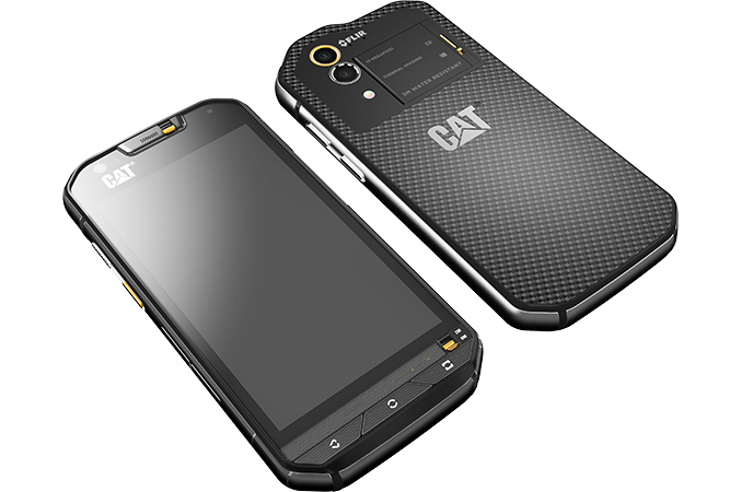
| 9:30a | CAT Announces S60 Rugged Smartphone with integrated FLIR Thermal Camera
CAT, that company that is usually associated with heavy machinery, actually makes/sells smartphones too. It has announced a new flagship smartphone, which combines the ruggedness you might expect from such a company with up-to-date functionality (Android 6.0) as well as an integrated thermal camera made by FLIR. The CAT S60 handset is designed for utility and construction workers as well as those, who work in harsh environments. Despite expectations, the smartphone will cost about the same amount of money as flagship devices from other manufacturers. Just like other CAT-branded smartphones designed by Bullitt Group (the company behind Cat Phones), the CAT S60 is rather bulky for good reason and is built on a die-cast stainless steel frame with carbon fiber inlays and a multitude of various details to ensure that the handset is dust- and water-proof. According to the developer, the smartphone can withstand drops onto concrete from up to 1.8 meters (MIL Spec 810G) and can even be used underwater (up to five meters depth) for one hour. The CAT S60 has special switches to block speaker and microphones when used underwater.
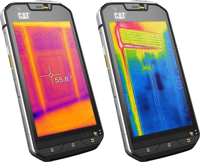
The key feature of the Cat S60 is its miniature thermal imaging camera based on the FLIR Lepton sensor (with 80×60 active pixels). The camera, which highlights temperature contrasts, can be used to identify over-heating electrical appliances and circuitry (or just check which computer components are the hottest ones and measure their actual temperature using a special application), detect heat loss around windows and doors, spot moisture and missing insulation and even see in complete darkness. The Cat S60 smartphone is based on the octo-core Qualcomm Snapdragon 617 system-on-chip (one block of eight ARM Cortex A53 cores up to 1.5 GHz, Adreno 405 graphics, a single-channel LPDDR3 memory controller, Wi-Fi, Bluetooth and an integrated X8 LTE modem with Cat 7 baseband capabilities) and Google Android 6.0 Marshmallow operating system. The handset features a 4.7” capacitive multi-touch display with 1280×720 resolution and improved brightness (540 nits), which is designed in such a way that it can be used while wearing gloves. The screen is protected with 1mm Gorilla Glass 4. The Cat S60 is also equipped with 3 GB of LPDDR3 memory, 32 GB of NAND flash storage (expandable using a microSD card), an underwater 13 MP main camera with dual-LED flash as well as a 5 MP front-facing camera, Wi-Fi, 4G LTE and Bluetooth wireless technologies, a host of sensors as well as a 3800 mAh battery. The phone can be connected to a PC or a charger using a micro-USB port.
CAT will demonstrate the S60 at Mobile World Congress and will make it available later this year for $599 in the U.S. or €649 in the E.U, although this is individual pricing and doesn't reflect the expected contract arrangements that might occur with larger businesses. Considering the fact that the smartphone more resembles a working tool than just a handset, its price does not seem to be too high, especially given that the smartphone thermal camera market is starting to take off (albeit at higher than 80x60 pixed quality). The fact that it is integrated rather than an add-on means it would get lost/broken less in a work environment. All that being said, the battery is non-removable (most likely due to the water proofing) and the dimensions/weight are unknown, but from the renders it might be more akin to a size of a larger 5.5-inch device and over 200g. Source: CAT (via Tech Report) Additional Reading | ||||||||||||||||||||||||||||||||||||||||||||||||||||||||||||||
| 10:00a | Samsung Portable SSD T3 Review Samsung launched the Portable SSD T3 at CES 2016. The claim to fame was the availability of 2TB of flash in a palm-sized enclosure with a USB 3.1 Gen 1 Type-C interface. The T3 builds upon the market success of the T1 released in early 2015. The T3 units are slated to become available in the market towards the end of February, but Samsung provided the press with early samples. Due to the rising popularity of USB 3.1 Type-C direct-attached storage (DAS) devices and the upcoming Thunderbolt 3 DAS units, we also took this review process as the opportunity to upgrade our core direct-attached storage testing platform. Read on for a detailed review of the 2TB Samsung Portable SSD T3 as well as the build log for our Skylake-based DAS testbed. | ||||||||||||||||||||||||||||||||||||||||||||||||||||||||||||||
| 7:01p | ARM Announces Cortex-A32 IoT and Embedded Processor
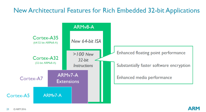
Today ARM announces the new Cortex A32 ultra-low power/high efficiency processor IP. For some readers this might come as a surprise as it's only been a few months since we saw the announcement of the Cortex A35 which was presented as a replacement for the Cortex A7 and A5, so this leaves us with the question of where the Cortex A32 positions itself against both past IPs such as the A7 and A5, but also how it compares against the A35.
The answer is rather simple: It's still a replacement for the A7 and A5, but targets even lower power use-cases than what the A35 was designed for. While ARM sees the A35 as the core for the next billion low-end smartphones, the A32 seems to be more targeted at the embedded market. In particular it's the "Rich Embedded" market that ARM seems to be excited about. The differentiation lies between use-cases which require a full-fledged MMU and thus able to run full operating systems based on Linux, and those who don't and could make due with a simpler micro-controller based on one of ARM's Cortex-M profile IPs. It's also worth to mention that although last time we claimed that the A35 would servce the IoT market, ARM seems to see wearables and similar devices as part of the "Rich Embedded" umbrella-term and thus now it seems more likely that it's the A32 that will be the core that will power such designs.
This leads us to the mystery of what exactly is the A32? During the briefing the only logical question that seemed to come to mind is: "Is this an A35 with 64-bit 'slashed off'?" While ARM chuckled at my oversimplification, they agreed that from a very high-level perspective that it could be considered as an accurate description of the A32. In more technical terms, the A32 is an 32-bit ARMv8-A processor with largely the same microarchitectural characteristics of the Cortex A35. As a reminder to our readers out there: The ARMv8 ISA is not only an 64-bit instruction set but also contains many improvements and additions to the 32-bit profile commonly named as AArch32. Among the larger differences between the A35 and A32 is that the latter's microarchitecture has been tuned and optimized to achieve the best performance and efficiency for 32-bit.
Indeed, performance wise, the A32 is advertised as being able to match the Cortex A35. The improvements lie in power efficiency: as a result of dropping its 64-bit capabilities, the new core is now able to achieve up to 10% better efficiency than the Cortex A35. Similarly to the A35, the A32 promises to achieve vastly superior performance per clock versus the Cortex A5 and A7, achieving anywhere from a 31% increase in integer workloads to a massive factor of 13x in crypto workloads, which the A32 is still capable of as they're included in the AArch32 ARMv8 profile.
While only a few months ago the Cortex A35 was advertised as ARM's smallest Cortex-A core, this title has now been passed on to the A32. ARM claims the core is around 30% smaller than the A35; The decrease in size, mostly due to the slimming down of the micro-architecture due the removal of 64-bit capability, allows the Cortex A32 to scale down to <0.25mm² in its smallest configuration, a significant decrease compared to the A35's disclosed <0.4mm². The core remains as configurable as the Cortex A35, able to run as either as single core or any as a cluster up to four cores. Optionally vendors can also configure cache sizes, with L1 ranging from 8KB to 32KB and L2 either being completely absent to up to 1MB in size. ARM's philosophy of "having the right design for the job" now seems more apparent than ever as we see an steadily increasing portfolio of processor IPs specialized for different use-cases. The A32 seems to fit right in with this strategy and we'll more than certainly see a large array of devices powered by the core in the future to come. | ||||||||||||||||||||||||||||||||||||||||||||||||||||||||||||||


| << Previous Day |
2016/02/22 [Calendar] |
Next Day >> |