[Most Recent Entries] [Calendar View]
Thursday, March 10th, 2016
- Rise of the Tomb Raider™(2)
- Up to 16% on AMD Radeon™ R9 Fury X Series vs AMD Radeon™ Software Crimson Edition 16.2.
- Gears of War Ultimate Edition(3)
- Up to 60% on AMD Radeon™ R9 Fury X series vs AMD Radeon™ Software Crimson Edition 16.2.1
- Up to 44% on AMD Radeon™ R9 380 series vs AMD Radeon™ Software Crimson Edition 16.2.1
| Time | Event | ||||||||||
| 12:30a | AMD Releases Radeon Software Crimson Edition 16.3 Hotfix: Support for Vulkan and TB3 Enclosures
With the driver update floodgates not closing yet, we are given a massive update from AMD that brings Radeon Software Crimson Edition to version 16.3 (driver version 16.15). Incoming this week is a good list of bug fixes, a large list of new features which include a couple of surprises, and some performance numbers to let us know how these cards have been improving. On the list of resolved issues, AMD has fixed an issue with cards not sustaining steady clock speeds, which had been leading to choppy performance. AMD also fixed a random crash in Rise of the Tomb Raider caused on launch of the game when Tessellation is enabled. And possibly most interesting of the fixes is the Ashes of the Singularity 2.0 Benchmark now supports DirectFlip, the absence of which limited AMD's ability to allow screen tearing for lower latency in that game. More significantly, a large number of features have been added to the driver and Radeon Settings application this time around. First is official support for Vulkan which AMD notes will bring the driver to Vulkan 1.0 compliance. Support has also been added for Per-Game Display Scaling. Which can be handy for those instances where a monitor or laptop may not always scale a game to fill the screen while not running at native resolution. In a new technology announcement, 16.3 adds support for what AMD calls XConnect technology. XConnect appears to be AMD's trademark name for supporting external Thunderbolt 3 GPU enclosures with Radeon R9 300 series GPUs, and includes supporting GPU plug’n’play. However AMD also notes that the base system will need to have BIOS support to connect to an external GPU, which implies that XConnect won't work with any and every TB3-equipped system. Finally, AMD also posted a list of performance numbers: While initially these are some stellar performance improvements, AMD states that the Tomb Raider numbers were tested at 1080p, while Gears of War Ultimate Edition was running at UHD (4K). These numbers also came from two different machines running different CPUs. Performance improvements are always good but internal validation has to be taken with a grain of salt, and a list this size can only give a small piece of the picture. As always, those interested in reading more or installing the updated hotfix drivers for AMD’s desktop, mobile, and integrated GPUs can find them either under the driver update section in Radeon Settings or on AMDs Radeon Software Crimson Edition download page. | ||||||||||
| 8:00a | Hands-On With the Android N Developer Beta: Multi-Window & More Yesterday Google surprised a number of people by launching the developer beta of the next release of Android, which is codenamed Android N. Normally the beta version of Android comes to developers during Google IO, but in a way it makes sense for Google to release it to developers a few months earlier so they can receive feedback and discuss common questions and concerns during the event. Read on for my early impressions of the latest version of Android. | ||||||||||
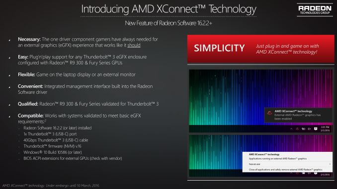
| 9:00a | More on AMD’s XConnect Tech: Thunderbolt 3 for External Radeons
Last night AMD issued a driver update that brought support for a new technology, XConnect. In a nutshell, XConnect is AMD’s trade name for running external video cards via Thunderbolt 3, a long awaited development that Thunderbolt owner Intel is finally getting behind and allowing. AMD’s driver release notes offered a handful of details, and now the official embargo for the tech is lifting, so we can fill in some of the blanks.
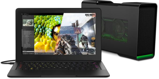
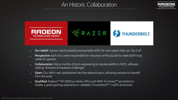
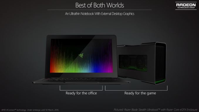
As our more observant readers may recall, when Intel unveiled Thunderbolt 3 back in June, they announced that they would finally be approving external video cards via Thunderbolt, and that they would be partnering with AMD to develop the initial implementation. More recently, at CES 2016 Razer unveiled the Razer Blade Stealth ultrabook, which was being immediately promoted as supporting external video cards, and was being shown off with its accompanying full power Core external video card chassis. Add the two up, and you can guess where this is going.
Today then is the formal launch of AMD’s Thunderbolt 3 video card efforts, which they are branding XConnect. The first drivers for XConnect were released last night, and now AMD is qualifying the Blade Stealth as the first laptop ready for XConnect. That said, it should be noted that while the Blade Stealth has been shipping for some time, Razer’s accompanying Core chassis has yet to ship, so anyone looking to try out XConnect will need to wait to get their hands on a Core.
Along with today’s formal unveiling of the technology, AMD is also laying out the technical requirements for supporting XConnect. Not just any laptop/desktop with Thunderbolt 3 can support an external GPU, as there are specific hardware and software requirements, which is why the Blade Stealth is the first qualified laptop. In particular, laptops need to support what is being called the Thunderbolt 3 external graphics standard, or eGFX for short. The eGFX standard in turn requires that vendors implement the necessary extensions for external graphics into their BIOS, including functionality necessary to support plug ‘n play operation. Also required is v.16 (or later) of the Thunderbolt firmware, Windows 10, and an active (not passive) Thunderbolt cable for bandwidth reasons. With all of the necessary parts in play, from a technical perspective what we’re looking at is a somewhat more complex AMD Enduro switchable graphics setup, except with an external GPU. XConnect allows for an external video card to feed either a laptop’s internal display via the normal switchable graphics protocols, or an external monitor hooked up to the external video card. I dare say that much of this is mundane in 2016 as switchable graphics have been with us for some number of years now, and Intel has told us as far back as June that what has really changed their tune was that there is finally a sensible GPU hotplugging solution in place, allowing video cards to be added and removed without rebooting. This makes it much easier to use an eGFX solution – hence AMD’s focus on plug ‘n play functionality – and it means the operating system won’t crash and burn if an external video card is removed. Though from AMD’s whitepaper it’s clear that applications using the external GPU will likely crash, which is why external video cards still should be ejected for best results.
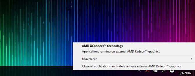
On the software side then AMD has gone ahead and implemented just this. The XConnect functionality in the latest Radeon drivers includes a system tray icon that that tells the user what applications are running on an external GPU, and can force close them if necessary to allow the GPU to be ejected/removed.
On the hardware side of matters, AMD is treating this as a high-end solution, and given the costs involved in Thunderbolt 3 I expect this will be the case universally. The company has qualified most of their high end graphics cards, including the R9 280, R9 290 series (sans 295X2), the R9 300 series, R9 Nano, and R9 Fury, while Fury X is excluded since its radiator won’t work with the Razor Core. Also supported are the mobile derivatives of these GPUs – for use in lower-power “graphics dock” devices – and future Polaris dGPUs will be supported as well. Overall from the GPU perspective Thunderbolt is just a higher latency PCIe 3.0 x4 connection, so it affords a lot of compatibility.
Meanwhile from a performance perspective AMD isn’t publishing specific numbers on how an external video card performs relative to an internal one, but PCIe 3.0 x4 testing is easy enough to do. With only one-quarter the bandwidth of a full PCIe 3.0 x16 slot Thunderbolt 3 will be constraining at times, but various benchmarks have put the average performance hit for a high-end card at under 10%. That of course will vary from game to game, as games that push a lot of data to the GPU or games that frequently interact with the GPU (e.g. retrieving physics simulation results) will be more greatly impacted by the reduced bandwidth and higher latency than simpler, more straightforward games. From a broader perspective, the launch of Razer’s Blade Stealth laptop and Core chassis are part of what AMD hopes will be a much larger ecosystem for eGFX-capable laptops and enclosures. While each end needs to be certified, the fact that the transport layer is standardized Thunderbolt 3 means that any chassis should work with any laptop, and future solutions need not be a matching setup ala the Blade Stealth + Core. To that end Thunderbolt eGFX is not the first external graphics solution, but as a standard it has the potential to be more widespread than previous proprietary solutions such as MSI’s Shadow expansion dock or AMD’s own previous XGP initiative, not to mention it’s not tied to any one GPU vendor. The catch, I suspect, will be getting laptop vendors to include Thunderbolt 3 support, as historically Thunderbolt has seen little traction outside of Apple laptops. The switch from the mini-Displayport connector to the USB Type-C connector is likely to help some with that, but a big consideration will be the space and power requirements of Intel’s Alpine Ridge controller, along with the costs of buying and integrating it.
As for the eGFX chassis, the Razer Core is a solid example of what to expect with high-end designs, which is a Thunderbolt dock on steroids. Along with providing enough power and space for a double-wide 375W video card, it also contains a Gigabit Ethernet port hanging off of the Thunderbolt controller’s PCIe lanes, USB 3.0 ports that are (presumably) coming off of the Alpine Ridge controller itself, and the ability to charge the Blade Stealth laptop. Back at IDF Intel was also pitching the idea for a smaller “graphics dock” concept, which would have a lower-power mobile-class dGPU integrated into a docking device that provided similar I/O functionality, to allow for a cheaper all-in-one device that provided a more modest boost to graphics performance. Overall, gaming has been one of the few bright spots in an otherwise sluggish PC industry, and that goes for both gaming desktops and gaming laptops. For AMD and Intel, the launch of Thunderbolt eGFX/XConnect in turn allows them to further expand the gaming laptop market, moving beyond desktop replacement class laptops and more limited 15” laptops by offering desktop-class GPU performance to any laptop that incorporates a Thunderbolt 3 port and the necessary BIOS support. At the same time Ultrabooks themselves have been a steady and well received market, though making poor gaming devices due to a lack of space for a dGPU – never mind something that offers desktop-like performance. So after earlier efforts to pair them up with external graphics with any luck this will be the start of a viable gaming Ultrabook market as well.
Gallery: AMD XConnect Presentation
      | ||||||||||
| 12:00p | Intel Updates True Key App to Simplify Security
Intel Security, a wholly owned subsidiary of Intel (and previously known as McAfee) has updated its True Key password manager application to tackle one of the most notorious issues with password managers: inability to reset the forgotten master password. The new version of the app allows resetting the master password using other methods of authorization. The updated version will simplify managing of passwords and will further help Intel in its quest to “eliminate” passwords in general. Since computing is getting increasingly mobile, security of personal devices is getting increasingly more important. As a major developer of PC platforms, Intel has created a number of sophisticated technologies that can improve security of computing devices. For example, Intel’s latest processors support AES-NI instructions that speed up encryption and decryption using the advanced encryption standard (AES). In addition, select Intel’s platforms also support TXT (trusted execution technology) and TPM (trusted platform module) cryptoprocessors for enhanced security. While strong passwords and AES 256-bit encryption can generally help to make mobile gadgets more or less secure, it is not easy to remember many strong passwords consisting of letters and numbers. Meanwhile, if you use only one password and it leaks, your security fails completely. It does not matter how sophisticated are encryption or security technologies, they get useless the moment when passwords are compromised. To make platform security technologies less vulnerable to human factor, Intel and some other companies want to eliminate passwords and replace them with more robust methods of authentication, such as fingerprints, retina scan or facial recognition. In fact, thanks to technologies like Apple Touch ID and Microsoft Windows Biometric Framework, usage of biometric authentication mechanisms instead of passwords as well as password managers to store passwords for applications that do not support biometric authentication is increasing.
Companies like IBM/Lenovo have offered password management for years with their ThinkVantage software, a proprietary program that only worked on their PCs. By contrast, Intel Security’s True Key password management application can work on various platforms; it is compatible with a variety of apps and can use different methods of authentication, including fingerprints, face, master password, trusted device, email and so on. For example, the True Key can use Intel’s RealSense cameras to recognize a face for Windows logon as well as third-party fingerprint scanners (i.e., Apple’s Touch ID). The Intel True Key always uses at least two factors to identify a person, which generally enhances protection, AES 256-bit encryption as well as Intel identity protection technology (IPT) where available. Since all biometric technologies are vulnerable to spoofing to some degree, True Key app allows biometric authentication only from the user’s own pre-selected trusted devices. Biometric templates for server-based facial recognition authentication (mathematical descriptions of biometric measurements) are stored on the True Key servers in encrypted form and are protected by a hardware security module (HSM). It should be noted that facial recognition is performed either completely in a server-based mode, or both on the user’s device and on the True Key servers. Meanwhile, the master password is not stored on True Key servers or locally on any device. It is used to generate the so-called key encryption key (KEK) as well as the authentication token (AT) using a large number of rounds of PBKDF2 with HMAC-SHA512 key derivation function with random salt values. The KEK is used to encrypt users’ passwords and wallet assets. The AT is used is used as one of the factors required to authenticate the user on the True Key servers.
The multi-factor authentication and the rather sophisticated master password make it very hard for perpetrators to access the data (simply because it takes too lot of codes to crack using brute force — even if someone manages to get the master password or crack KEK and AT, they will also have to crack another method of authorization). Whenever the master password is changed, the True Key re-encrypts all data both locally and on servers. What is very important for many users is that Intel’s latest version of the True Key can reset even the master password by verifying other unique factors like owner’s face and/or fingerprint via a second device. So, even if you forget something, the application can relatively safely reset everything, which should simplify its usage for many people. Intel’s True Key application supports Apple Mac OS X, Google Android and Microsoft Windows operating systems as well as Internet Explorer (Edge), Google Chrome and Mozilla Firefox browsers. Free version of the program supports up to 15 passwords, premium version can store up to 2000 logins and passwords for $19.99 a year. | ||||||||||
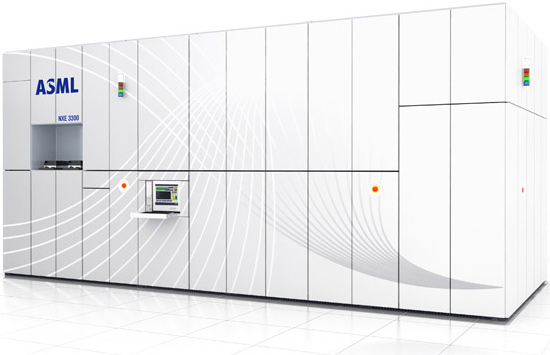
| 3:00p | EUV Lithography Makes Good Progress, Still Not Ready for Prime Time
At the recent annual SPIE Advanced Lithography conference, Intel, TSMC and other leading semiconductor companies said that significant strides have been made in extreme ultraviolet lithography (EUVL) over the past year or so. Intel did not reveal when exactly it plans to start using EUV technology, but indicated that it will clearly utilize it once it is suitable for high-volume production of semiconductors and is sufficiently cost effective . Samsung and TSMC also intend to start inserting EUVL tools into production in the coming years. Chip Production Gets HarderAs chipmakers transit to newer process technologies every several years, sizes of transistors and electronic circuits within microprocessors shrink, making them more complex and powerful, but also harder to manufacture using traditional photolithographic methods. Feature sizes of today’s circuits within modern chips can be as small as 42 nm, whereas modern semiconductor production tools use deep ultraviolet (DUV) argon fluoride (ArF) excimer lasers with 193 nm wavelength. To compensate for this difference, Intel and other makers of advanced chips use multiple techniques to enhance resolution of photolithographic equipment.
One of the key transistor density improving technologies is immersion lithography, which replaces the air gap between the lens and wafer with liquid, whose refraction index is higher than one. For example, purified deionized water has refraction index of 1.44 and this allows to enhance resolution of production tools by up to 40% depending on materials. Another key tech for contemporary semiconductor manufacturing is called multiple patterning, a semiconductor production technique that allows to increase feature density by resolving multiple lines on the same photoresist layer using multiple photomasks. Usage of multi-patterning essentially means that certain layers within one chip are exposed multiple times, which greatly increases complexity of manufacturing operations and stretches production cycles, essentially increasing costs of chips. Intel has been using multi-patterning since mid-2000s and its 65 nm manufacturing technology. The technique did not cause a lot of troubles at first, but things got very complicated with the 14 nm fabrication process because the number of mask steps significantly increased compared to previous-gen technologies. Meanwhile it is taking the company longer to develop its 10 nm manufacturing process, tune its designs and achieve high yields than it used to be, which is why the company had to delay its Cannonlake CPUs from 2016 to 2017. It's also important to note that Intel's 14nm process introduced air gap dielectric in certain interconnect layers, which dramatically increased the number of engineering problems to overcome as introducing voids into the interconnect leads to structural instabilities that must be controlled appropriately. Basically, as it becomes increasingly tougher to develop new manufacturing technologies and produce modern chips using currently available tools, the benefits of node-to-node transitions shrinks, which is rather dangerous for chipmakers from an economic standpoint. In order to address negative effects of multi-patterning, producers of step and scan systems used in semiconductor manufacturing significantly increased output of such tools, as well as enhanced their resolution and boosted their overlay and focus performance. For example, ASM Lithography (ASML), the world’s largest maker of scanners, claims that its latest TWINSCAN NXT:1980Di can process up to 275 wafers per hour and can be used to make chips using sub-10 nm process technologies. While such scanners will be utilized going forward, with so many mask steps required, a new method of photolithography will make far more sense. EUV Makes a Big Promise, But Generates Big ChallengesEUV lithography, whose development started in 1985 and which used to be called Soft X-Ray, utilizes extreme ultraviolet wavelength of 13.5 nm. Using EUV can greatly enhance the feature density of chips without heavy reliance on multi-patterning and additional layers. For example, TSMC can produce 46 nm metal pitches with a single exposure, an operation that requires usage of four masks for an ArF scanner. Moreover, Intel has managed to produce wafers with 22 nm metal pitches using its own micro EUV tool. Among other advantages, EUV is expected to shrink cycle times and promises to increase yields of chips at advanced nodes. Unfortunately, EUV is an extremely complex technology that not only requires all-new step-and-scan systems for production of semiconductors, new chemicals and new mask infrastructure, but it is also so tricky to use that its actual resolution can end up far below expectations.
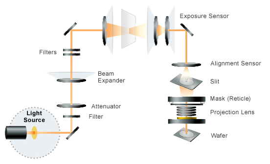
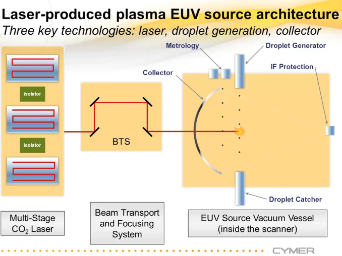
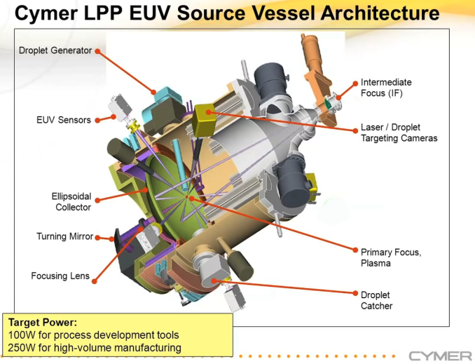
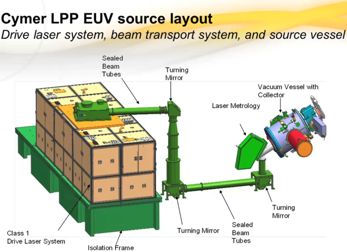
It should be noted that generation of EUV light is a rather difficult process itself. Cymer, a division of ASML that produces light sources for lithography tools, is developing laser produced plasma (LPP) EUV sources. The LPP technology applies CO2 laser to small tin droplets (which are around 30 microns in diameter), creating ionized gas plasma at electron temperatures of several tens of electron volts. The 13.5 nm radiation is then collected by a special ~0.5 meter mirror coated with several layers of molybdenum (Mo) and silicon (Si), in order to selectively reflect the maximum possible amount of 13.5 nm EUV light and direct it to the Intermediate Focus (IF) position at the entrance to the scanner system.
To put it simply: in order to generate 13.5 nm EUV light in a special plasma chamber, you need a very powerful laser (because a significant amount of its power will be wasted); a generator and a catcher for tin droplets (in addition to a debris collector); as well as a special, nearly perfect, elliptical mirror. To make everything even trickier, since EUV light with 13.5 nm wavelength can be absorbed by almost any matter, EUV lithography has to be done in vacuum. This also means that traditional lenses cannot be used with EUV because they absorb 13.5 nm light; instead, specialized multilayer mirrors are used. Even such mirrors absorb about 30% of the light, which is why powerful light sources are needed. This level of absorption can lead to ablative effects on the mirrors themselves, which introduces additional engineering challenges. To learn more how EUV LPP light sources work, check out this video.
The 13.5 nm EUV light generator needs to have a powerful light source that can expose economically viable amount of wafers per hour (or day). One of the key issues with the TWINCSCAN NXE scanners was that is their laser produced plasma EUV source was not powerful enough. Until recently, performance of experimental EUV equipment from ASML, such as the TWINCSCAN NXE:3300B scanners, was limited to around 500 wafers per day due to power source limitations. By contrast, the current-generation TWINSCAN NXT scanners can process from 175 to 275 wafers per hour (which is good enough, considering heavy usage of multi-patterning). The reliability of the droplet generator was mediocre just about a year ago. Moreover, lifetime of the collector mirror is a yet another point of concern due to the previously mentioned ablative effects.
Things Are Getting BetterThe progress of EUVL scanners as well as EUV source systems has been steady in the recent years. ASML, which is one of the major driving forces for extreme ultraviolet lithography, recently said it had hit multiple stability, availability and productivity targets in 2014 and 2015 and is optimistic about the future. According to ASML, in 2015 one of the company’s clients managed to expose more than 1000 wafers per day on the NXE:3300B, whereas ASML itself managed to hit 1250 wafers per day milestone on the NXE:3350B. ASML also said that it could operate a 200 W light source for one hour with full dose control. For HMV (high volume manufacturing) equipment, 250 W light sources will be needed. ASML is not sure when such light source will be made, but it hopes to hit this milestone in 2016 or 2017. Hence, there is still a long way to go for suitably powerful EUV light sources.
At the SPIE Advanced Lithography conference, Intel confirmed that there were four running EUV tools with 80 W light sources around the world as of early 2016, up from one a year ago. Intel itself now uses the NXE:3300B tool with Cymer’s 80 W EUV sources on its 14 nm pilot line for 21 hours per day, leaving three hours for engineering and servicing. Britt Turkot, senior principal engineer in logic technology development lithography at Intel, said that experimental EUV production had demonstrated good overlay trends, stable critical dimension uniformity as well as good electrical testing and end-of-line yield results. Another piece of good news is that the reliability of the tin droplet generator also improved significantly over the past year. Intel indicated that the tin droplet generator now achieves 85% of its expected lifetime. Reflectivity of the elliptical collector also degrades in accordance with expectations. ASML and Intel are also seeing combined scanner and source availability (4-week rolling average) exceeding 70%, which is good enough for development, but is still unacceptable for mass production. ASML plans to increase availability of its tools to 80% this year.
EUV Photomask Industry Needs Further DevelopmentExtreme ultraviolet lithography no longer uses lenses and traditional glass photomasks (reticles), but utilizes specialized mirrors as well as multi-layer reflective photomasks. Even a minor defect in a photomask makes it unusable because it affects the final wafer. To discover such defects, makers of photomasks or chips can use currently available optical mask inspection tools, e-beam/multi e-beam tools (which are slow) or actinic patterned mask inspection tools, the latter of which have not been commercialized yet. For now, optical mask inspection tools based on 193 nm or other wavelengths can be used for EUV photomasks, but there is a problem. Since photomasks (reticles) in extreme ultraviolet lithography are even more vulnerable than conventional glass photomasks, they can be easily damaged by falling particles during exposure or even by 13.5 nm EUV light itself. To address this issue, Intel and ASML have been working collaboratively to add a special pellicle to protect the photomask. Protective films for EUV should be extremely thin, should not affect reflection characteristics of photomasks, and should sustain EUV power levels. Unfortunately, it is impossible to use currently available 193 nm mask inspection tools like scanning or tunneling electron microscopes to review an EUV reticle with a pellicle on it, according to SemiEngineering and industry sources. Only actinic patterned mask inspection (APMI) tools are useful for this purpose. However, the latter are not available today outside of academic labs like Berkeley's SHARP mask imaging microscope. As a result, semiconductor companies had to invent a way for mask shops to inspect reticles without pellicles using contemporary equipment and then install protection before shipping masks to fabs (which means that it will be impossible to inspect photomasks after the fact at fabs using current tools). According to the world’s largest CPU maker, its pelliclized reticles can sustain over 200 wafer exposures. However, defectivity levels on such pellicle membranes are still high, which means that flaws can essentially affect wafers and dramatically lower yields. Moreover, it remains to be seen whether producers can supply enough of such membranes. What is even more important is that to inspect reflective photomasks for EUVL, chipmakers will still need actinic patterned mask inspection equipment. Without such tools and timely repair of photomasks using e-beam tools, yields will inevitably become an issue, Intel has said. Since APMI tools do not exist today (even though KLA-Tencor is said to be developing such devices), it will take years before they reach the market. Moreover, such equipment will not be cheap, they will resemble scanners and will require EUV light sources. At the SPIE conference, Intel demonstrated successful defect mitigation strategies on multiple devices, and a healthy e-beam pattern defect repair capability. So, the situation with mask inspection and repairs is improving, according to the CPU maker. EUV Is Required for 7 nm Technology, But Will Be Implemented “When It’s Done”In general, the industry remains rather optimistic about EUV lithography thanks to two years of solid progress. All leading makers of semiconductors, including Intel, TSMC, Samsung and GlobalFoundries plan to use EUV tools as soon as it makes sense. All four chipmakers indicated on various occasions in the recent months that EUV lithography will be required for 7 nm manufacturing technology. At the SPIE conference, TSMC and Samsung re-affirmed plans to insert EUVL into 7 nm production. By contrast, Intel indicated that while it would prefer to use EUVL for critical layers at 7 nm, it would only use the tech when it is completely ready. At present, Intel is experimenting with EUV on its 14 nm pilot fab line and the results have been encouraging, according to the company. Nonetheless, Intel believes that to make EUV a reality, in addition to many other things, the industry needs to improve yields, decrease costs and develop an ecosystem of EUV photomasks. Finally, while step-and-scan systems with EUV's 13.5 nm wavelength will help to produce microprocessors and other chips using 5 nm and, perhaps, 7nm, technologies, contemporary 193nm ArF tools are not going anywhere. Virtually all chipmakers say that EUV scanners will only be used for critical layers of chips. For layers that can be produced using multi-patterning, DUV tools will be used.
Intel, TSMC and Samsung have publicly said that they plan to start producing chips using their 10 nm manufacturing technologies in 2017. These process technologies have already been developed without EUV, and unless the chipmakers decide to introduce new versions that involve EUV for critical layers, EUV will continue to not be used for 10 nm. The leading makers of semiconductors are currently finalizing their 7 nm technologies this year, and they will have to make decisions regarding usage of EUV tools with their 7 nm nodes in 2018 – 2019, according to Peter Wennink, CEO of ASML. If currently available EUV tools meet expectations of chipmakers, they will order production TWINSCAN NXE systems and will use them two or three years down the road. Sources: Intel, Semiconductor Engineering, Semiconductor Manufacturing and Design, SemiWiki. | ||||||||||


| << Previous Day |
2016/03/10 [Calendar] |
Next Day >> |