[Most Recent Entries] [Calendar View]
Tuesday, March 22nd, 2016
| Time | Event | ||||||||||||||||||||||||||||||||||||||||||||||||||||||||||||||||||||||||||||||||||||||||||||
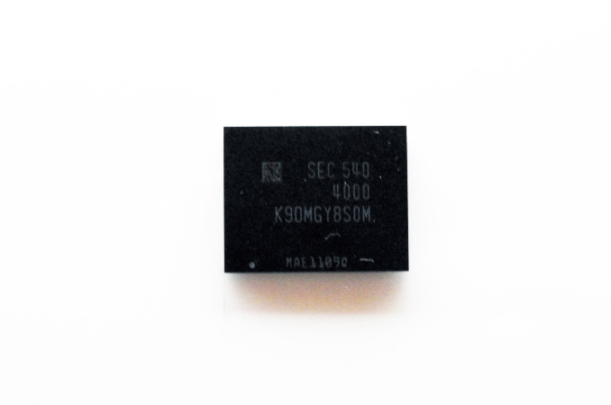
| 8:00a | Samsung Demos Its First BGA SSD: 1500 MB/s Read Speed and Tiny Package
In the recent years SSDs in M.2 form-factor have greatly reduced the amount of space required for storage sub-systems inside modern PCs. However, as computers get even smaller, there is pressure for SSDs to further shrink as well. Solid-state drives in BGA packaging are considerably smaller than SSDs in M.2 form-factor and for a couple of years platform developers like Intel have been promoting such drives among PC makers. Intel said in 2014 that an M.2-2260 SSD could take 15% of space inside a 2-in-1 hybrid PC, whereas usage of a BGA SSD could save a great amount of space and could allow to increase battery size by around 10%. Moreover, in many cases usage of BGA storage can shrink Z-height of devices as well as improve thermal performance compared to M.2 modules, according to Intel. As a result, the market for BGA form factor SSDs has been growing in size and importance at a quick pace. To that end, at the 2016 Samsung SSD Forum Japan, Samsung demonstrated its first SSD in a BGA (ball-grid array) packaging. Despite of tiny form-factor, Samsung’s PM971 SSD offers rather high performance thanks to PCIe interface and a special controller. Meanwhile the little drive will be targetted for use inside PCs, tablets, 2-in-1s and other types of small computers or embedded applications. First BGA SSD From SamsungSamsung’s PM971 SSD is based on Samsung’s new Photon controller as well as MLC V-NAND flash memory. It is impossible to say at this time whether the Photon controller of the PM971 SSD has anything to do with the controller used inside the 750 EVO drives (the controller is smaller than usual as it has only two processing cores), but it looks very likely.
At the event, Samsung did not reveal anything about internal architecture of its BGA SSD, which is rather interesting because the NAND controller has to extract maximum performance out of a limited number of NAND devices over a limited number of channels (provided, of course, that internal architecture relies on industry standards). Moreover, it is unknown whether the drive is compatible with the proposed M.2 specification for BGA SSDs. The only thing that is known about the SSD right now is that it is smaller than an SD card, according to PC Watch web-site. Samsung is aiming for tablets and 2-in-1 hybrid PCs with its BGA SSDs, The company expects device manufacturers to adopt the product in the second half of 2016 or in the first half of 2017. Standards for BGA SSDs ProposedWhile we're on the subject of BGA SSDs, this is a good time to touch upon the recent developments in the standardization of SSDs in this format. Even with the recent growth of the market, SSDs in BGA packaging are not something completely new. Intel, Toshiba, SanDisk, Microsemi, Silicon Motion and some others have all offered SSDs in BGA form-factors for years to various makers of embedded applications, whom in turn needed to save space or run their storage sub-systems in harsh environments. Early last year Toshiba rolled-out its first BGA SSDs with PCIe interface, and in September several members of PCI SIG (the organization, which develops PCIe interface, its derivatives and standards for PCIe-based devices) proposed a set of mechanical standards for BGA SSDs, which could open the doors for many manufacturers to enter the emerging market.
BGA SSDs with PCIe 3.0 or SATA interfaces will be a part of the PCI SIG’s M.2 specifications. At present select members of the organization (HP, Intel, Lenovo, Micron, SanDisk, Seagate and Toshiba) propose four types of soldered-down solid-state storage solutions: Type 1620, Type 2024, Type 2228 and Type 2828. M.2 types traditionally define width and length of the package in millimeters, so, the smallest BGA SSD will have measurements of 16 × 20 mm, whereas the largest BGA SSD will feature 28 × 28 mm packaging. SSDs in a BGA package may have Z-height up to 2 mm (measured with solder balls collapsed), but may be slimmer. BGA SSDs that comply with the proposed M.2 types use the same signals as the M.2 socket 3 (so, they are compliant with both PCIe 3.0 and SATA 3.2 protocols and can utilize up to four PCIe lanes), but use 1.2V, 1.8V and 3.3V power rails. All the BGA SSDs contain the common core ball map of Type 1620 (which look pretty much the same as the core ball map of Toshiba’s BG-series SSDs) for data and power, but the larger drives also feature additional mechanical retention balls. Some BGA SSDs can be placed on M.2 modules in a bid to enable design flexibility for device makers (and upgradeability option for end-users), but only on the condition that the modules have voltage conversion circuitry to provide 1.8V or 1.2V as required.
A BGA SSD not only integrates NAND flash memory, but also a NAND controller, DRAM and all the things that could be needed for a fully-functional solid-state storage solution. From the software perspective, M.2 spec BGA SSDs are just solid-state drives with PCIe or SATA interfaces. And unlike MCPs (multi-chip packages) consisting of DRAM and NAND that companies like Micron and Samsung offer to makers of mobile devices, BGA SSDs are complete storage systems that can be attached directly to appropriate host interfaces. The proposed BGA M.2 form-factors intend to unify packaging of single-chip SSDs and make such SSDs industry-standard devices available from various makers. It is unknown at this time whether Samsung’s PM971 will be compliant with the proposed specs, but it's worth noting that the company is a member of PCI SIG and typically makes products in standard packages and form factors. | ||||||||||||||||||||||||||||||||||||||||||||||||||||||||||||||||||||||||||||||||||||||||||||
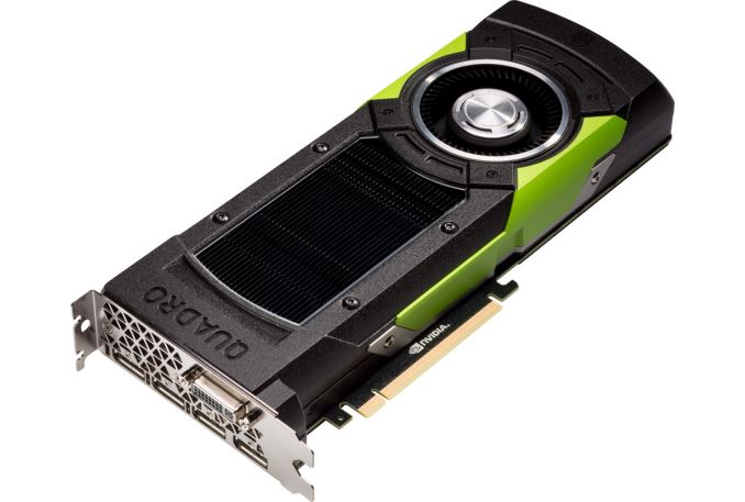
| 9:00a | NVIDIA Announces 24GB Quadro M6000
With NVIDIA currently between GPU generations, things have been relatively quiet on the professional graphics front for the company. On the high-end NVIDIA released the Quadro M6000 back in 2015, bringing their fully enabled GM200 GPU into the professional market. Now just over a year later, they are giving the Quadro a refresh with a newer, higher capacity model.
When the original Quadro M6000 was launched, NVIDIA outfitted it with 12GB of VRAM in a 24x4Gb configuration, a large amount of memory for the time but not the full amount a GM200 card could be equipped with. Now this week the company is giving the card mid-cycle upgrade by increasing its VRAM capacity, replacing the 12GB model with a 24GB model utilizing higher density 8GB GDDR5 memory chips. The target market for the 24GB M6000 is relatively straightforward: certain segments of the professional visualization market need all of the VRAM they can get, so for NVIDIA ecosystem users this should be a welcome upgrade. At the same time since 8Gb GDDR5 has been on the market for some time now, I’m surprised it has taken NVIDIA this long to bring GM200 to its maximum 24GB capacity. None the less this does give NVIDIA bragging rights as the highest capacity professional graphics card – surpassing the 16GB FirePro W9100 – though it’s worth noting that AMD should have the capability to push that to 32GB if they want final bragging rights.
Meanwhile NVIDIA’s press materials also briefly note that the updated Quadro M6000 ships with some new temperature & clockspeed management options – presumably via a newer firmware – though details are limited. The new M6000 features "More discrete GPU clock options for a better customer experience when running their application" and "Greater software temperature control to keep the GPU temperature below the hardware slowdown threshold for the best user experience.” NVIDIA’s professional cards (Quadro & Tesla) feature more performance controls than we see on consumer cards (which just run as fast as they can) and from the description I expect that NVIDIA has put in some new, finer grained options to better control automatic throttling behavior by manually setting both the maximum clockspeed and temperature. For single card workstations this is rarely an issue, but for large arrays of cards (e.g. Quadro VCA), keeping all of the cards in lockstep with regards to performance is a desired feature. Finally, since this is a mid-cycle refresh, the new 24GB Quadro M6000 will be launching this week. It will be a drop-in replacement in NVIDIA’s product stack, and will occupy the previous M6000’s spot at $5000. | ||||||||||||||||||||||||||||||||||||||||||||||||||||||||||||||||||||||||||||||||||||||||||||
| 11:30a | Andrew S. Grove, Former CEO and Chairman of Intel, Passes Away Aged 79
It is our sad news today to extend a report that Andy Grove, a Silicon Valley pioneer and the former CEO and chairman of Intel, passed away aged 79. Mr. Grove joined Intel the day it was incorporated in 1968 and left active roles at the company in late 2004. Andy Grove played a critical role in Intel’s decision to refocus from computer memory to microprocessors in the eighties. He was also behind Intel’s transformation into a widely recognized consumer brand. Born to a middle-class Jewish family in Budapest, Hungary, his family immigrated to the U.S. when he was 21, having survived Nazi occupation and escaping Soviet repressions. In the U.S. he studied chemical engineering at the City College of New York and then completed his Ph.D. at the University of California at Berkeley in 1963. Andy started his industry career at Fairchild Semiconductor, a pioneer in the manufacturing of integrated circuits, where Gordon Moore hired him as a researcher. By 1967, he became assistant head of R&D. At Fairchild, Mr. Grove developed a variety of integrated circuits and worked with such legendary engineers as Robert Noyce, Jerry Sanders and many others. When Intel was founded in 1968, Andy was Intel’s third employee and started as the director of engineering, getting Intel’s manufacturing operations off the ground. Over the course of his career at Intel, Andy wrote several textbooks on the topics of semiconductors and management, some being used at a university level, as well as over forty technical papers and holds several patents. In 1979 Andy was Intel’s President, being made CEO in 1987, overseeing a growth in revenue to $20.8 billion at the time. In 1997 he became Intel’s Chairman, relinquishing his role as CEO in 1998 and continuing on the board until 2004 while working as a senior advisor to Intel and a lecturer at Stanford. He was Time magazine’s Man of the Year in 1997. During his tenure as the chief executive, he made two important business decisions for the history of Intel. Firstly, he started to withdraw from the market of DRAM in the eighties because of heavy competition from Japanese makers. While Intel was larger than its rivals, it could not compete against all of them and instead of trying to pick an important market segment, it was decided that this was a moment for the company to refocus its business in general. Eventually, he described the process and decisions behind it in his book “Only the Paranoid Survive.” Secondly, he initiated massive CPU-related ad campaigns for consumers, which led to the Intel Inside brand to make the importance of microprocessor technology evident to the mainstream public. The decision to advertise CPUs beyond the pre-installed systems led to transformations of the semiconductor industry and to a degree helped expand the DIY PC market we know today. This led to Intel responsible for everything related to its CPUs. Thus when in 1994 it was discovered that the original Pentium processor had a fundamental bug in its FPU, the company replaced processors and organized the whole replacement scheme itself, which cost millions of dollars. Nonetheless, the company solved all the issues with the original Pentium chip under Mr. Grove's tenure. During Andy’s time at Intel, being a staunch advocate of open and honest debate and direct lines of communication to senior management, he oversaw a large portion of the super-fast growth in personal computing through the 1980s, 1990s and into the new century. It’s clear how much his work has had an effect on the computing industry and here at AnandTech. Anand started the website as a hobby back in 1997, the same year Andy became Chairman, and since then we’ve always been enthusiastic about the progression of personal computing as well as the enterprise segment, areas which Andy and Intel have steered into something completely unimaginable over 40 years ago.
The legacy of Mr. Grove will carry on, both as a brilliant pioneer of the semiconductor age but also in the components and devices we use. While not a household name like Moore, Jobs or Gates, Grove stands among them (with Dennis Richie) in the annals of computing. | ||||||||||||||||||||||||||||||||||||||||||||||||||||||||||||||||||||||||||||||||||||||||||||
| 4:15p | Google Updates Youtube For iOS To Support Slide Over And Split Screen
Today Google shipped an update for the Youtube application on iOS. The update brings the app to version 11.10, and it's one of the more significant updates the app has seen since Google brought the interface over from the Android version after the last major redesign. With this update the app now supports iOS 9's split screen and slide over multitasking on iPads. Both features work in the same way as other applications. While slide over is just a by-product of supporting split screen, it's probably not too useful due to the fact that you can't continue playback in the background when you slide the app away again. On the other hand, split screen is very handy for watching a video while doing something in another application. It is a bit awkward in a sense because if you try to make the video full screen it has really large black bars on the top and bottom, but that's just due to the app aspect ratio when multitasking. All that's left now is for Google to include support for Picture in Picture windows. This would be the pinnacle of convenience, as it would let you watch the video even when the Youtube app isn't actually on screen at all, and it would just sit in a perfectly sized floating window. There are probably a few of reasons why PiP still isn't supported, including API limitations and difficulty with displaying advertisements and targeting using cookies, but it's hopefully something Google is working on. For now, iPads users can grab the updated Youtube for iOS from the App Store and try out the new multitasking capabilities. | ||||||||||||||||||||||||||||||||||||||||||||||||||||||||||||||||||||||||||||||||||||||||||||
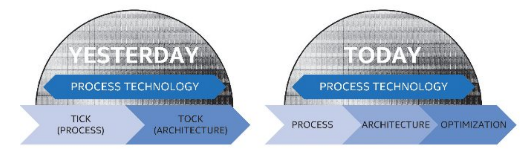
| 6:45p | Intel’s ‘Tick-Tock’ Seemingly Dead, Becomes ‘Process-Architecture-Optimization’
As reported at The Motley Fool, Intel’s latest 10-K / annual report filing would seem to suggest that the ‘Tick-Tock’ strategy of introducing a new lithographic process note in one product cycle (a ‘tick’) and then an upgraded microarchitecture the next product cycle (a ‘tock’) is going to fall by the wayside for the next two lithographic nodes at a minimum, to be replaced with a three element cycle known as ‘Process-Architecture-Optimization’ Intel’s Tick-Tock strategy has been the bedrock of their microprocessor dominance of the last decade. Throughout the tenure, every other year Intel would upgrade their fabrication plants to be able to produce processors with a smaller feature set, improving die area, power consumption, and slight optimizations of the microarchitecture, and in the years between the upgrades would launch a new set of processors based on a wholly new (sometimes paradigm shifting) microarchitecture for large performance upgrades. However, due to the difficulty of implementing a ‘tick’, the ever decreasing process node size and complexity therein, as reported previously with 14nm and the introduction of Kaby Lake, Intel’s latest filing would suggest that 10nm will follow a similar pattern as 14nm by introducing a third stage to the cadence.
From Intel's report: As part of our R&D efforts, we plan to introduce a new Intel Core microarchitecture for desktops, notebooks (including Ultrabook devices and 2 in 1 systems), and Intel Xeon processors on a regular cadence. We expect to lengthen the amount of time we will utilize our 14nm and our next generation 10nm process technologies, further optimizing our products and process technologies while meeting the yearly market cadence for product introductions. While the new PAO or ‘Performance-Architecture-Optimizat
Intel’s current fabs in Ireland, Arizona, and Oregon are currently producing wafers on the 14nm node, with Israel joining Arizona and Oregon on the 22nm node. Intel also has agreements in place for third-party companies (such as Rockchip) to manufacture Intel’s parts for certain regional activity. As well as looking forward to 10nm, Intel’s filing also states projects in the work to move from 300mm wafers to 450mm wafers, reducing cost, although does not put a time frame on it. The manufacturing lead Intel has had over the past few years over rivals such as Samsung, TSMC and Global Foundries, has put them in a commanding position in both home computing and enterprise. One could argue that by elongating the next two process nodes, Intel might lose ground on their advantage, especially as other companies start hitting their stride. However, the research gap is still there - Intel introduced 14nm back in August 2014, and has since released parts upwards of 400mm2, whereas Samsung 14nm / TSMC 16nm had to wait until the launch of the iPhone to see 100mm2 parts on the shelves, with Global Foundries still to launch their 14nm parts into products. While this relates to density, both power and performance are still considered to be on Intel’s side, especially for larger dies.
Intel's Current Process Over Time On the product side of things, Intel’s strategy of keeping the same microarchitecture for two generations allows its business customers to guarantee the lifetime of the halo platform, and maintain consistency with CPU sockets in both consumer and enterprise. Moving to a three stage cycle has thrown some uncertainty on this, depending on how much ‘optimization’ will go into the PAO stage: whether it will be microarchitectural, better voltage and thermal qualities, or if it will be graphics focused, or even if it will keep the same socket/chipset. This has a knock on effect with Intel’s motherboard partners, who have used the updated socket and chipset strategy every two generations as a spike in revenue. Suggested Reading: EUV Lithography Makes Good Progress, Still Not Ready for Prime Time | ||||||||||||||||||||||||||||||||||||||||||||||||||||||||||||||||||||||||||||||||||||||||||||


| << Previous Day |
2016/03/22 [Calendar] |
Next Day >> |