[Most Recent Entries] [Calendar View]
Friday, March 25th, 2016
| Time | Event | |||||||||||||||||||||||||||||||||||||||||
| 8:00a | More Than Throughput: Next Generation Wi-Fi Testing with Ixia's WaveDevice It’s been quite some time since I first started writing for AnandTech, and without question there’s been a lot of changes that have happened to our testing methodologies in the past few years. One of the main issues that I’ve always been thinking about while working through reviews is how we could improve our testing methodology in a meaningful way outside of simply updating benchmarks to stay current. Internally we’ve been investigating these issues for quite some time now, and these changes have included the addition of SoC power efficiency comparisons and display power efficiency measurements. There are a lot of other changes here and there that I still want to make, but one of the major unexplored areas has been wireless radio performance. Wireless performance testing is probably one of the hardest things that we could test, and for a time I had almost given up hope on deploying such testing within AnandTech. However life has a way of playing out differently than I expect, and in the past few months we’ve been working with Ixia to make Wi-Fi testing a reality. Ixia, for those of our readers who aren't familiar with the company, is a traditional player in the networking test space. They are perhaps best known for their Ethernet test products, and more recently have been expanding into wireless and security testing with the acquisition of companies like VeriWave and BreakingPoint Systems. We have done Wi-Fi testing before, but in the past we were mainly focused upon a relatively simple and arguably not particularly interesting test case: maximum throughput in ideal conditions. It was obvious that Wi-Fi in many devices is still not perfect, as subjective differences in reception and reliability can feel obvious. However, without any data or methods of replication it was hard to really prove that what we felt about wireless performance was really the case. To see how we've changed this, read on for the full article. | |||||||||||||||||||||||||||||||||||||||||
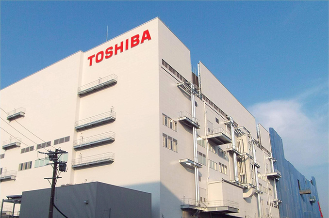
| 9:00a | Toshiba to Build New Fab to Produce BiCS NAND Flash
Toshiba this month has announced plans to build a new manufacturing facility to produce its BiCS NAND flash memory. The company intends to start making chips at the new fab in 2018 and currently is not disclosing the planned production capacity of the factory. SanDisk yet has to confirm its participation in building the new fab, but the announcement itself means that despite an ongoing financial scandal, Toshiba is set to remain one the world’s largest makers of NAND flash memory. Toshiba plans to invest around ¥360 billion ($3.233 billion) in its new facility in fiscal 2016 to fiscal 2018, with that price tag covering both construction costs and equipment investments. The fab will be located on land adjacent to the Yokkaichi Operations memory production complex in Mie prefecture, which means that the company essentially wants to add a new production complex to its Fab 5 (which is currently produces 2D NAND) and Fab 2. Exact decisions regarding construction schedule, manufacturing tools and other will be made in Toshiba’s fiscal 2016, which begins in April. Construction of a semiconductor manufacturing facility usually takes about a year. After the building is complete inside and outside, it takes about two or three quarters to move in equipment and start volume production. Therefore, Toshiba’s plan to begin operating the new facility in fiscal 2018 (which begins on April 1, 2018) seems viable.
The new fab will solely produce Toshiba’s 3D NAND memory, which the company calls BiCS (Bit Cost Scalable) NAND. Toshiba claims that the architecture of its proprietary BiCS NAND is more efficient in terms of die sizes compared to other types of 3D NAND thanks to its U-shaped NAND string. So far independent analysts have not verified whether Toshiba’s 48-layer 256 Gb TLC BiCS NAND chips are smaller or larger than Samsung’s 48-layer 256 Gb TLC V-NAND ICs, but if this proves to be the case, then Toshiba will enjoy lower production costs over time. Meanwhile at present, Toshiba and SanDisk already operate multiple fabs for non-volitile memory, including the world’s largest NAND flash manufacturing facility, Fab 5 (phases 1 and 2) at the Yokkaichi Operations memory production complex in Mie Prefecture. Ahead of their newly announced fab for 2018, Toshiba and SanDisk are scheduled to produce their BiCS NAND memory at both Fab 2 and Fab 5 over the next year. BiCS production at Fab 2 is set for the first half of FY2016 (i.e., from April to October, 2016), and SanDisk has previously indicated that it would begin conversion of some of the capacity in Fab 5 to 3D NAND in 2016. Keeping in mind that SanDisk cannot do anything in the fab alone, it is clear that Toshiba and SanDisk have a plan to gradually convert the fab to 3D NAND in the future.
If Toshiba’s plan succeeds, by the second half of calendar 2018 it will have several semiconductor manufacturing facilities capable of producing BiCS NAND memory. While the combined manufacturing capacities of all three fabs are unknown at the moment, it is likely that the company will continue to produce vast amounts of NAND flash memory. Toshiba said that it expected to continue its joint venture operation with SanDisk in expanding BiCS Flash capacity in the new facility. However, SanDisk is being acquired by Western Digital at the moment and it remains to be seen on what terms the new company will join Toshiba in investments. Together, Toshiba and SanDisk currently make and sell more flash memory than Samsung, but keeping in mind how aggressively the latter plans to expand its semiconductor manufacturing capacities in the coming years, everything is subject to change. Last year Samsung announced plans to invest an additional $9.2 billion in expansion of its manufacturing facility near Pyeongtaek, South Korea. The latter will cost Samsung $14.4 billion and is scheduled to begin operations in 2017. While the fab is officially intended for DRAM production, its vast manufacturing capacities could be used to produce other types of semiconductors as well. | |||||||||||||||||||||||||||||||||||||||||
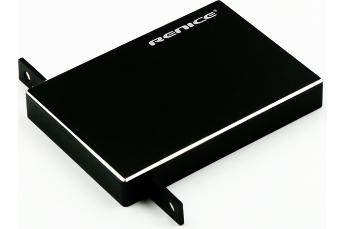
| 12:00p | Renice Announces X9 Military-Grade Rugged SSDs with R-SATA Connectors
Shenzhen Renice Technology, a little-known maker of special-purpose SSDs from China, has introduced its new family of drives designed for military and rugged applications. What makes these new drives notable is that they are designed to withstand harsh environments, utilizing special R-SATA connectors as well as custom controllers. On the NAND side the drives are build around SLC, MLC or pseudo-SLC NAND flash memory to provide the required balance between endurance, price and performance. The Renice X9 R-SATA SSDs are powered by the company’s own controller, the RS3502-IT, as well as SLC or MLC NAND flash memory from undisclosed manufacturers. The drives are made in accordance with the MIL-STD-810F spec to withstand harsh environments and poor handling, and feature integrated power failure protection as well as 256-bit AES encryption with several secure erase functions (both software and hardware). The Renice X9 SSDs use the company’s proprietary 15-pin R-SATA connectors as well as special 7-pin SATA power ports, which limits compatibility of the drives to applications that feature the same connectors.
The SLC-based X9 R-SATA drives are offered in 128 GB – 1 TB configurations, whereas MLC-powered SSDs are available with 256 GB – 2 TB capacities. If required, Renice can use MLC NAND in pseudo-SLC mode in order to provide higher endurance and performance at a predictable cost. The Renice X9 comes in 2.5” form-factor with 7, 9 or 15 mm thickness, depending on the exact capacity configuration. The manufacturer claims that the X9 SSDs have maximum sequential read speed of up to 530 MB/s and maximum sequential write speed of up to 500 MB/s along with 0.1 ms access time. The company does not specify random read/write performance of the drives, but claims that it is “excellent”. Keeping in mind that X9 SSDs can use different types of NAND flash memory and come in various configurations, random I/O performance of different models is likely to vary greatly.
With regards to reliability, the Renice X9 drives boast a MTBF of over four million hours, while their physical tolerance is rated for 16.4G (10 – 2000 Hz) sustained vibration and 1500G (@ 0.5 ms half sine wave) shock, something that typical drives simply do not offer (Intel's DC S3710 SSD, by comparison, can tolerate 2.17 G operating vibration and can survive 1000 G shock). The X9 SSDs are designed for operating temperatures ranging from -40°C to +85°C (industrial-grade) or even -55°C to+125°C (military-grade), which is in line with other SSDs for extreme environments (such as those from Amtron or Foremay). Meanwhile, datacenter drives like the DC S3710 can operate when its temperature is between 0ºC and +70ºC.
Given that Renice is a Shenzhen-based company, it is admittedly unlikely that the X9 SSDs will be used in military or defence applications outside of China. Nonetheless, since the drives are designed to withstand harsh environments in general, the X9 SSDs can be used in aerospace, industrial, transportation, outdoor storage and other systems that are subject to extreme temperatures, severe vibrations and other types of harsh environments. Exact pricing of the Renice X9 depends on memory configuration and additional features that the manufacturer may offer (e.g., extended operating temperatures). Typically, rugged drives cost significantly more than typical SSDs. | |||||||||||||||||||||||||||||||||||||||||


| << Previous Day |
2016/03/25 [Calendar] |
Next Day >> |