[Most Recent Entries] [Calendar View]
Thursday, March 31st, 2016
- 16 MB buffer
- 5400 RPM spindle speed
- SATA III 6 Gbps interface
- Stylish industrial design for the aluminum enclosure gives it a premium look and feel (tying in closely with the LaCie branding message)
- Redesigned setup process for the average consumer base to be able to use the drive with both Mac and Windows systems.
- Changes in bundled features and software
- Replacement of the micro-B USB 3.0 port with a Type-C USB 3.1 Gen 1 port capable to delivering up to 5 Gbps of throughput
- Photos: 15.6 GB collection of 4320 photos (RAW as well as JPEGs) in 61 sub-folders
- Videos: 16.1 GB collection of 244 videos (MP4 as well as MOVs) in 6 sub-folders
- BR: 10.7 GB Blu-ray folder structure of the IDT Benchmark Blu-ray (the same that we use in our robocopy tests for NAS systems)
- Adobe Photoshop (Light)
- Adobe Photoshop (Heavy)
- Adobe After Effects
- Adobe Illustrator
| Time | Event | |||||||||||||||||||||||||||||||||||||||||||||||||||||||||||||||||||||||||||||||||||||||||||||||||||||||||||||||||||||||
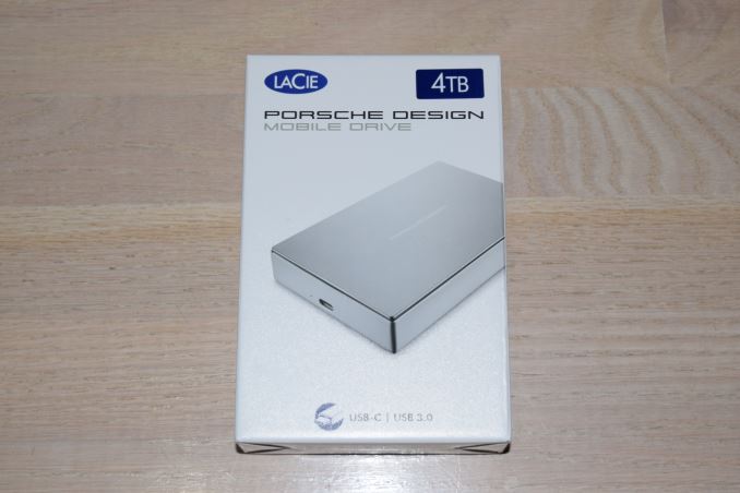
| 8:00a | LaCie Porsche Design Mobile Type-C External HDD Capsule Review
Seagate launched a host of direct-attached storage products under the LaCie brand name at CES earlier this year. Though the LaCie Chrome USB 3.1 Gen 2 Type-C external SSD was easily the most impressive announcement of the lot, it is the LaCie Porsche Design Mobile which is making it to the market first. The unit started shipping last week. Once the review unit reached our hands, it was easy to see why. It turns out that the internal drive is the Seagate / Samsung Momentus ST4000LM016, the same as the one we saw in the Seagate Backup Plus Portable last year. This 2.5" drive has a 15mm thickness, making it suitable for use in bus-powered external drive enclosures.
Important aspects of the drive include: It appears that the ST4000LM0016 uses five platters with a 800GB/platter design to achieve the capacity point. The USB 3.0 bridge chip also supports UASP and S.M.A.R.T passthrough. The LaCie Porsche Design Mobile 4TB version has dimensions of 128 mm x 84 mm x 21 mm and weighs 315 grams. It comes with a quick start guide, as well as a USB 3.1 Gen 2 Type-C to Type-C cable (rated for SuperSpeed USB 10 Gbps) and a Type-C to Type-A cable.
Compared to the Seagate Backup Plus Portable, the Porsche Design Mobile P9227 external hard drive brings the following updates: The industrial design of the unit is in line with what we have come to expect from LaCie's product lines designed by Porsche Design. The enclosure is fully aluminum and the contours are quite pleasing. The product presents a premium look and targets LaCie's traditional consumer market quite nicely. Thanks to the bundled Type-C to Type-A cable, the product is compatible with both traditional USB Type-A and the new Type-C ports. Setup ImpressionsThe product's setup process is optimized for consumers who are not particularly tech-savvy, and don't want to be bothered with partition tables and other such things. Upon connecting to a computer, a 260MB FAT32 partition with the LaCie setup program gets mounted.
The Windows setup program allows the end-user to configure multiple partitions, if necessary, for use with multiple operating systems (FAT32 for Windows, Mac and Linux, and NTFS for Windows). The bundled software suite includes Genie Timeline Free (a backup software for Windows) and LaCie's Desktop Manager (a configuration / management software for LaCie devices in the local network). The gallery below presents some of the other options in the setup process. DAS BenchmarksThe LaCie Porsche Design Mobile P9227 4TB drive was formatted in NTFS for our benchmarking process. In order to evaluate the DAS aspect of the unit, we utilized the testbed outlined in the table below to test the performance. One of the USB 3.1 ports enabled by the Intel Alpine Ridge controller was used to connect the unit to the system.
Our testing methodology for DAS units takes into consideration the usual use-case for such devices. The most common usage scenario is transfer of large amounts of photos and videos to and from the unit. The minor usage scenario is importing files directly off the DAS into a multimedia editing program such as Adobe Photoshop. Prior to taking a look at the real-life benchmarks, we first check what ATTO and CrystalDiskMark have to report for the LaCie Porsche Design Mobile P9227.
In order to tackle the first real-life use-case, we created three test folders with the following characteristics:
The above benchmark run was also instrumented to record the drive temperature as well as instantaneous transfer rates during the process. The internal disk temperature was only slightly more than 40 C even after more than 127 GB of writes and 127 GB of reads continuously.
For the second use-case, we take advantage of PC Mark 8's storage bench. The storage workload involves games as well as multimedia editing applications. The command line version allows us to cherry-pick storage traces to run on a target drive. We chose the following traces. Usually, PC Mark 8 reports time to complete the trace, but the detailed log report has the read and write bandwidth figures which we present in our performance graphs. Note that the bandwidth number reported in the results don't involve idle time compression. Results might appear low, but that is part of the workload characteristic. This is not the intended use-case for portable hard drives, but the results are just presented here for the sake of completeness.
Power ConsumptionEvaluation of the power consumption of the drive was done using Plugable's USBC-TKEY. Our test procedure and setup are outlined here.
The drive idled at around 2.12 W, while the peak power consumption was 4.05 W. So, it might be a prudent idea to not operate the drive off a bus-powered hub in case there are other USB peripherals sharing power from the same port. Concluding RemarksThe LaCie Porsche Design Mobile P9227 external hard drive continues LaCie's tradition of bringing a premium look and feel to top-of-the-line PC and Mac accessories. The industrial design of the unit is definitely praiseworthy. Consumers who value aesthetics and a premium look/feel for their computing accessories might want to give the LaCie Porsche Design Mobile drive a try. In addition, the Type-C interface ensures that the drive can be easily used with Type-C-only devices such as the MacBook. Power delivery is not applicable to the Porsche Design Mobile, since the unit is bus-powered. The externally powered desktop version supports USB-PD, though. The bundled Type-C to Type-A cable ensures that the drive can work equally well with any legacy USB port also. The LaCie Porsche Design Mobile P9227 4TB is currently available on Apple.com for $230. The other option for consumers looking for a 4TB bus-powered portable drive is the Seagate Backup Plus Portable 4TB version which is currently on sale for $120. In addition to having the same performance for real-life workloads (the drive inside both the units are the same, after all), the Backup Plus Portable also comes with some add-on software features such as Lyve and 200GB of online cloud storage for 2 years. Without doubt, the Backup Plus Portable provides the best value for money. However, LaCie's target market for the Porsche Design Mobile drive is unlikely to give much weight to the value proposition aspect. | |||||||||||||||||||||||||||||||||||||||||||||||||||||||||||||||||||||||||||||||||||||||||||||||||||||||||||||||||||||||
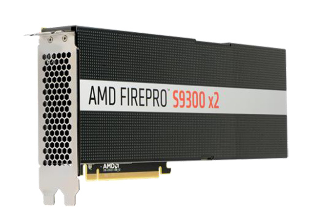
| 9:00a | AMD Announces FirePro S9300 X2: Dual Fiji for HPC
One of the more interesting consequences of GPUs being built on TSMC’s 28nm process for an extended period of time is that it has forced both vendors to compensate and compromise in order to have product lines that cover the nearly 5 year span. Traditional upgrade cycles got thrown out of the window, and instead we saw a number of refreshes and updates, culminating in both AMD and NVIDIA taking their top GPUs right to the 28nm reticle limit of ~600mm2. Such large GPUs have typically been the crossover point between graphics and compute parts, incorporating high-end features such as ECC memory and faster double precision (FP64) compute capabilities. However for the reticle riders, AMD and NVIDIA went another route, building what is arguably the ultimate graphics GPUs with the highest FP32 performance possible. I mention this because it puts the GPU vendors into the position of doing unconventional things with their GPUs. Nowhere is this more evident than in the new FirePro card AMD is announcing today. The FirePro S9300 X2 is the latest entry into the FirePro S series lineup, and it marks the first (and possibly only) time we’ll see AMD’s Fiji GPU used to power an HPC-grade compute card. The end result is an interesting product that at times will be wickedly powerful for a 300W card, and at other times will have to cope with the abilities and limitations of a GPU that wasn’t designed for the traditional HPC market.
As alluded to by the name, the S9300 X2 is a dual Fiji card, integrating a pair of AMD’s last and most powerful 28nm GPUs. In the interests of delivering a more efficient 300W card, AMD clocks S9300 X2’s GPUs at 850MHz, giving the card a theoretical 13.9 TFLOPs of FP32 compute performance. Meanwhile on the memory side AMD leaves the card’s HBM memory untouched, with each GPU getting 512GB/sec of memory bandwidth, for an aggregate 1TB/sec of bandwidth. Like its graphics counterpart, the Radeon Pro Duo, the S9300 X2 is designed to be the fastest thing available in a single card, at least for the niche where Fiji shines. Since making its consumer debut nine months ago, I have been pondering whether AMD would attempt to deploy Fiji in a FirePro card. Fiji is arguably built for graphics first and foremost; its FP64 performance is capped at 1/16th FP32 performance, it lacks ECC memory, and its limited to just 4GB of memory per GPU. Given the expectations set by “traditional” HPC cards such as the FirePro S9170 – which offers 4-8x the memory and 3x the FP64 performance – Fiji seemingly can’t stack up. However in building the ultimate graphics GPU, AMD also built the ultimate FP32 compute GPU – one that on paper delivers far more FP32 performance than any other HPC card – and this is where the company will be running with this card. The end result is that the S9300 X2 is an interesting niche product designed for a certain market segments that need strong FP32 performance above all else – and everything else held equal, don’t use massive data sets. It’s a somewhat narrow niche as a result, but one AMD believes they can do very well in given what kind of FP32 performance S9300 X2 is capable of, especially as NVIDIA doesn’t have an FP32 HPC-focused dual-GPU card of their own.
If you follow the HPC market then the market segments AMD is going after should sound familiar to you. Oil and gas (geosciences) has long been a FP32-centric field – something NVIDIA exploited a few years back as well with the Tesla K10 – and AMD will be chasing after this market with the S9300 X2. AMD will also be trying to push farther into the neural network market, and this is an area where the S9300 X2 may be uniquely suited. Popular GPU neutral network implementations don’t use FP32 math, rather they use even lower precision FP16 math. And though the S9300 X2’s FP16 throughput is merely equal to its FP32 throughput, internally Fiji supports natively storing FP16 data types, which will significantly reduce register pressure on the card, and register pressure is almost always a concern for HPC kernel development.
AMD will also be looking to exploit the products of their Boltzmann Initiative – now formally called the Radeon Open Compute Platform (ROCm) – which will be near or at production quality by the time the S9300 X2 ships. With AMD’s newest card providing the necessary muscle at the hardware level, the company is looking towards ROCm’s heterogeneous compiler to close the gap with NVIDIA on the software side, with the HIPify tools to further bridge that gap by giving developers the means to port their CUDA applications over to AMD’s platform. AMD has already seen some success with ROCm with the geosciences firm CGG, and they’re hoping to continue this trend as the ROCm platform reaches production quality.
Wrapping things up, when it’s released the S9300 X2 will take its place alongside the rest of AMD’s FirePro S series lineup. Continuing to ship alongside it will be the S9100 series cards, which are based on AMD’s Hawaii GPU and compliment the S9300 X2 with traditional HPC-centric features such as ECC memory and high performance FP64. The FirePro S9300 X2 will be shipping this quarter with an MSRP of $5999. Gallery: AMD FirePro S9300 X2 Press Deck
      | |||||||||||||||||||||||||||||||||||||||||||||||||||||||||||||||||||||||||||||||||||||||||||||||||||||||||||||||||||||||
| 11:41a | Intel Cloud Day 2016 Live Blog, 9AM PT I'm here at Intel's Cloud Day at the Nasdaq Center in San Francisco, ready for a live blog of the keynote talk from Diane Bryant, SVP and GM of Intel's Data Center Group. It is set to start at 9AM PT. | |||||||||||||||||||||||||||||||||||||||||||||||||||||||||||||||||||||||||||||||||||||||||||||||||||||||||||||||||||||||
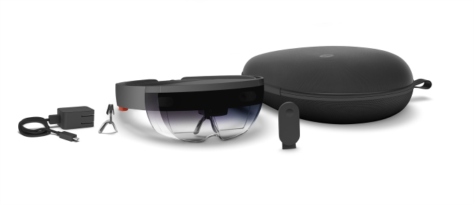
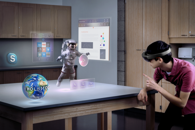
| 11:50a | Hololens Round Two: Augmented Reality At Build 2016
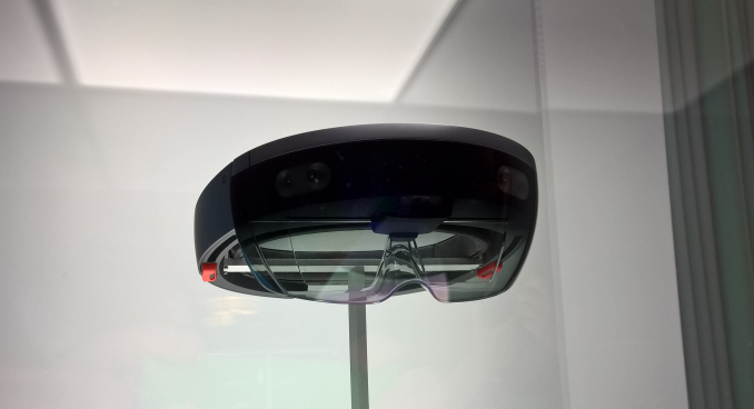
Last year at Build I got my first chance to try Hololens. That experience was very interesting, not only because of the potential of Augmented Reality, but the entire circus surrounding the device. The Hololens sessions were at a different location, and the groups brought over had to lock up everything electronic. We could only do photos of a unit in a display case. Naturally when Microsoft announced yesterday that Hololens would start shipping to developers yesterday, this year’s experience could never be so secret. So when we got to the demo location, and were given keys for a locker, I was a bit taken aback. But it wasn’t anything as sinister this time, only a way to make sure there were no backpacks on the floor as tripping hazards, because this year’s untethered experience was really untethered.
That comes a bit later though. This year’s demo involved building and deploying an 3D app using Unity and Visual Studio, and each person doing the demo also got a coach to help solve any issues on the way. The Hololens unit was slightly different this year, but looking at it, it was remarkably similar to last year’s demo version. The one big change this year was very welcome. Instead of having a person physically measure the inter-pupillary distance on your head (the distance between your pupils), the experience is now handled through software when you first put the headset on. There is a quick calibration that you can run and it sets your eye position based on some air tap gestures. It was very quick and easy, and the set walks you through everything required with voice and visual cues. Then we sat down building our apps. Since this was a demo for press, all of the coding was done ahead of time and we just had to walk through adding scripts in Unity to set up the demo. Then we build them, and deploy to a remote machine using the IP address of the Hololens. The demo app was of an energy ball which, when locked to a location in space, would open up and show some nifty effects. The experience was very basic compared to what I would expect of the retail apps, but this was a simple demo and it worked well. The very interesting bit was later on, when we linked our Hololens units with the other people in our pods of six people. This way all six people could interact with a single energy ball. People also got to choose an avatar which would float over their heads. That experience was pretty amazing. With very little setup, the holograms were truly linked to a single point that all people could see. As part of this demo, my coach suggested I walk around the (very large) room and then look back. This was probably the most amazing part of the demo. After walking a hundred feet or more away, and around some tables and pillars, I looked back and the hologram was still floating exactly where I left it. The ability to really lock things to a location is really the one part that needs to be perfect for this experience to work, and they really nailed it. In addition, my pod mates were all around the room with avatars floating over their heads. So with a night to think about it, here are my thoughts after using the Hololens a year later. The field of view issue is still very small, and clearly not something they were not able to address before they shipped to developers. I would explain it as something like a mid-sized television, in the 27-inch range, sitting a few feet away from you. My experience was better this time because there were less software issues, but the small field of view can certainly take some getting used to. The hardware itself was very easy to put on and adjust, and it was fairly well balanced in that I never felt like the unit was heavier on the front where the lenses are. The adjustment is done with a wheel on the back, much like a welding helmet if you’ve ever seen one of those. The right side has buttons for volume, and the left side has buttons for brightness. I had to crank up the audio quite a bit because of the loud room we were in, and although the audio was spatial, it was hard to get a sense of that with the commotion going on during the demos. Although I don’t wear glasses, it looked like there would be no issues wearing glasses with it, and several of the other attendees seemed to have no issues putting the device on and using it with them. The experience of AR is much different than VR. Because you are interacting with things in real space, you can easily move around without fear of tripping or walking into a wall. VR is able to offer much more powerful graphics and immersion right now, but you are largely bound to a single location. The use cases for AR seem, to me, to be not necessarily the same as VR and both should easily be able to co-exist.
While doing my demo, I asked my coach how to close the app we were running, and he showed me a “bloom” gesture which closes it. Once I did that, I was in another mode for the Hololens where I could see how it mapped out the physical world with polygons by tapping my finger in a direction. This was amazing and the Hololens did a great job on picking up everything in my area, including the people, with no issues. I then did another bloom and was back at the start screen. On the demo units, this was pretty sparse, but I was able to go into settings and play around. I didn’t see anything special in there other than the process of interacting with the menus was very simple and was very easy to get used to. From a UI aspect, the Hololens did very well. At the end of our demo we did some shooting of orbs which opened up a hole in the floor. Peering down into it, it really felt like this was something you didn’t want to step into. The holograms tend to be a bit translucent, but on this one in particular it was much more solid. There’s a lot of untapped potential here and I hope to get a chance to do some of the other demos they have here to get a better feel for that. The headset itself seemed to be near the edges of its processing power on the final demo though, which had a lot of not very complex polygons moving around, and the six people interacting. There was a lot of things to keep track of, as well as quite a few holograms flying around. Microft then said that all of the code that we used in the demo, and all of the code used on the demos last year, is all available on GitHub to allow devs quicker access to code. I think the Hololens is still one of the most interesting pieces of tech I’ve used in a long time. There is a lot of potential here for education, training, and even tasks like painting your house and trying different color samples. There are quite a few applications where this would work very well.
The hardware though still needs a bit of work. It is a bit bulky, and the lenses would not stay anchored to the spot in front of me where I set them, so I had to readjust. The field of view is also not very large, and this could be because the processing power is not as powerful as the tethered experiences of VR. I look forward to seeing where this goes in the future. A lot of the pieces are already well done and on the software side, the experience is very good. With a bit better hardware, which will almost certainly come with time, this is going to be a very powerful tool from Microsoft. | |||||||||||||||||||||||||||||||||||||||||||||||||||||||||||||||||||||||||||||||||||||||||||||||||||||||||||||||||||||||
| 11:59a | Microsoft Announces Xamarin Will Be Included Free With Visual Studio, And Open Source
Back in February, Microsoft announced it was acquiring Xamarin, the cross-platform toolkit which allows developers to write native apps for iOS, Android, Windows, and Mac, using Visual Studio and C# code. Today during the Build day 2 keynote, Scott Guthrie announced Xamarin will now be included for free with all editions of Visual Studio, and Xamarin will join the rest of .NET in being made open source. Previously Xamarin was an expensive set of tools, and while powerful, the cost was prohibitive to a lot of developers. By moving the Xamarin tools right into Visual Studio at no cost, Microsoft is making a play to have Visual Studio be a much better platform for coding on all platforms.
Xamarin outputs native apps for the supported platrforms, and as part of the demo, Microsoft showed off a new feature of Visual Studio which is a remote simulator for iOS. Since they can’t emulate iOS directly on Windows like they can with Android, this at least allows you to debug and run apps in real-time without having to switch computers. | |||||||||||||||||||||||||||||||||||||||||||||||||||||||||||||||||||||||||||||||||||||||||||||||||||||||||||||||||||||||
| 12:30p | The Intel Xeon E5 v4 Review: Testing Broadwell-EP With Demanding Server Workloads Fifteen months after first reaching consumers, Broadwell has finally arrived in the server space with Broadwell-EP. Premiering with the Xeon E5 v4 family, Intel is now offering server processors with up to a staggering 22 cores. Of course, there is much more to discuss than just a higher core count in the Xeon world. Join us as we introduce you to the a new killer enterprise application, brand new real world benchmarks on top of the latter, and our usual benchmarks on no less than five different generations of Xeons!
| |||||||||||||||||||||||||||||||||||||||||||||||||||||||||||||||||||||||||||||||||||||||||||||||||||||||||||||||||||||||
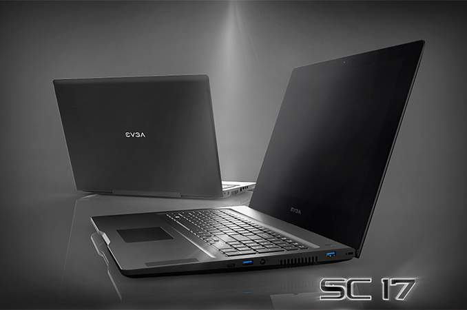
| 3:00p | EVGA Rolls Out SC17: High-End Gaming Laptop Designed for Overclocking
EVGA this week officially introduced its SC17 laptop designed for demanding gamers, which combines rather high performance with UHD display. The system features an Intel Core i7 microprocessor with unlocked multiplier, a high-end NVIDIA GeForce GTX graphics adapter, a combination of fast and capacious storage devices as well as a 4K display Two key features of the system are its ability to fine-tune microprocessor’s voltages in a bid to maximize overclocking potential as well as GPU overclocking support. The EVGA SC17 laptop was designed by the company’s engineers completely in-house in a bid to offer functionality not available on other high-end notebooks. While EVGA is primarily known for its video cards and motherboards, keep in mind that that the company hired engineering team from Epox, a legendary maker of mainboards for enthusiasts, sometimes in mid-2000s (in fact, Andrew Han, a co-founder of EVGA, was also a co-founder of Epox), and thus has a lot of experienced talent when it comes to platform development. As a result, the EVGA SC17 sports a fully-fledged UEFI BIOS, which gives users control over many aspects of system’s performance, including CPU voltages, memory timings and so on. In fact, even the GPU can be overclocked from the BIOS, which is not a feature that you can typically find on notebooks. For those, who want to get maximum out of their systems, there is even a “clear CMOS” button on the chassis in order to reset settings in case of a malfunction. For users, who do not want to hevaily tweak their PC, the SC17 supports EVGA Express OC (EOC) technology that lets to easily overclock the system to gain performance, or downclock it to prolong battery life, with a press of two button.
EVGA’s new gaming laptop is based on the Intel Core i7-6820HK processor (four cores with Hyper-Threading, 2.70 GHz/3.60 GHz frequency, 8 MB L3 cache, HD Graphics 530, 45 W TDP) with unlocked multiplier, which was designed with overclocking in mind. The SC17 notebook is also equipped with NVIDIA’s GeForce GTX 980M graphics processing unit with 8 GB of GDDR5 memory, 32 GB of G.Skill’s DDR4-2666 memory, a 256 GB M.2 SSD with NVMe protocol (PCIe 3.0 x4 interface) as well as a 1 TB hard drive with 7200 RPM spindle speed. Just like other high-end laptops, the EVGA SC17 sports a full-HD webcam, built-in speakers with subwoofer, a Gigabit Ethernet controller, a IEEE 802.11ac Wi-Fi + Bluetooth 4.2 module, one USB 3.1 type-C port, two USB 3.0 ports, mDP as well as HDMI display outputs and so on.
EVGA’s engineers remained loyal to their overclocking origin and incorporated a rather advanced cooling system with two fans and eight vents into the SC17. The cooling system is designed to ensure that the Core i7-6820K and the GeForce GTX 980M receive enough cool air even when they are overclocked. It should be noted that NVIDIA is not particularly enthusiastic about mobile GPU overclocking these days, meaning EVGA would have had to do some extra work to offer this for customers.
Another important aspect of the EVGA SC17 is its 17.3” display. The 4K (3840×2160) screen is based on an IPS panel by Sharp. It is unknown whether Sharp has applied its IGZO backplane technology to the panel to make for better power efficiency but it's a reasonably fair bet given the display size and resolution. EVGA’s SC17 should offer performance levels comparable to good gaming PCs featuring Intel’s Core i7 “Skylake” CPU as well as NVIDIA’s GeForce GTX 970 GPU. This should be enough not only for mainstream gaming, but also for VR gaming, something that may be interesting to many people these days. Despite of rather high performance, the SC17 is not too bulky or heavy: it is 1.05” (26.9 mm) thick and weighs 3.69 kilograms (8.14 pounds), which is low compared to many other 17” notebooks.
While EVGA this week officially introduced the laptop, it did not reveal when exactly it plans to start selling it, but expect the mobile PCs to arrive in the coming weeks. The price of the notebook in the default configuration is $2699.99, which is not very high given the unlocked Core i7 processor as well as the GeForce GTX 980M inside. | |||||||||||||||||||||||||||||||||||||||||||||||||||||||||||||||||||||||||||||||||||||||||||||||||||||||||||||||||||||||
| 8:00p | Intel Rolls Out New PCIe SSDs for Cloud Datacenters
Intel on Thursday introduced several new PCIe SSDs designed for cloud datacenters. The new drives increase capacities, shrink latencies and offer higher throughput in order to follow demands of new datacenters deployed by various companies these days. Some of the new SSDs are based on Intel’s 3D NAND memory, whereas other feature NVMe 1.2 technology and dual-port U.2 capability to increase performance of mission-critical data-storage applications. Intel hopes that in the future SSDs will be used not only to store hot, frequently used data, but also data that is currently stored on highly-reliable high-performance hard drives. To replace 10K and 15K RPM HDDs in the datacenter, Intel needs to offer improved reliability, high endurance, unbeatable performance, lower costs and additional features impossible on HDDs. The new SSDs from the company bring a number of improvements to the datacenter compared to previous-generation drives.
The new Intel SSD DC P3320 and P3520 families of SSDs are based on 32-layer 3D NAND flash memory developed and produced by Intel and Micron. The drives are powered by unspecified controllers, and support end-to-end data protection as well as some other functions important in the datacenters. Intel claims that that its 3D NAND has better endurance than planar NAND flash memory, which is common knowledge at this point, but does not provide any exact numbers for their NAND. The DC P3320 comes in 2.5” or HHHL card form-factor and uses either PCIe 3.0 x4 or U.2 to connect to the host. The DC P3320 is being pitched as a step up from Intel's SATA-based datacenter SSDs, while the DC P3520 will presumably be replacing the DC P3500 series.
The DC P3320 SSDs offer a range of capacities, including 450 GB, 1.2 TB and 2 TB models and are designed for read-intensive applications. The new drives are rated to offer maximum sequential read/write speed of up to 1600/1400 MB/s. Maximum random 4K read/write speed declared by Intel for the DC P3320 is 365K/22K IOPS (input/output operations per second). Intel does not reveal any details about the DC P3520, but claims that these drives were designed to deliver “significant” performance and latency improvements over the DC P3320 (which probably indicates higher parallelism and higher capacities, which Intel does not want to talk about at the moment).
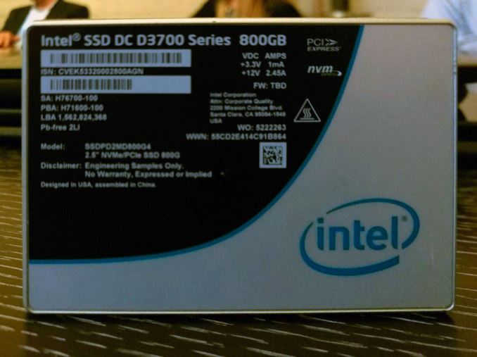
Meanwhile the new Intel DC D3600/3700 SSDs (not to be confused with the P or S series) are designed for mission-critical storage applications that should function 24/7, which is why they utilize proven MLC NAND flash memory with high-endurance technology (HET) as well as controllers that support NVMe 1.2 technology with various high-availability features and support for up to 80 I/O queues. Intel does not disclose which controller it uses, but claims that they feature an integrated memory buffer and dynamic multiple namespaces management technology to improve efficiency of data management across drives in one machine, an exclusive feature (which potentially means that Intel uses a custom controller for these SSDs). The drives sport an active/active dual-port design that connects through a compatible backplane to two host systems simultaneously (which enables run-time recovery during failover when one of the hosts is unavailable) and support hot-plug capability. The DC D3600/D3700 drives also feature end-to-end data protection, power-loss data protection with self-test and thermal throttling and monitoring to ensure maximum reliability. The SSDs utilize PCIe 3.0 x4 interface and U.2 connectors. Since each drive has only a single U.2 connector, their dual-port mode relies on the backplane routing two PCIe lanes to each of the two host systems.
Intel’s DC D3600/D3700 solid-state drives will be available in 800 GB, 1.6 TB (D3700) as well as 1 TB and 2 TB (D3600) configurations. According to Intel, the new SSDs, deliver sequential read speeds of up to 2100 MB/s and sequential write performance of up to 1500 MB/s. The new SSDs can also perform up to 470K random read IOPS (4KB) and up to 95K random write IOPS (4KB). Since SSDs with U.2 interface are not compatible with existing SAS or SATA backplanes (because they do not support PCIe), they need support from makers of storage solutions for datacenters. Intel claims that companies like EMC, Huawei, Quanta, Wistron and X-IO Technologies are ready to produce mission-critical storage ecosystem for PCIe-based SSDs, but does not provide further details. A hands-on look at a sample of the DC D3700 revealed that Intel has changed the design of the heatsink on the bottom of the drive to allow for airflow in two directions across the back half of the drive where the controller most likely resides.
Intel did not touch upon price and availability details about its new SSDs, but expect them to arrive later this year. Keeping in mind that there are not a lot of mission-critical PCIe backplanes in the wild at the moment, it will take some time before Intel’s DC D3600/D3700 get more or less widespread. | |||||||||||||||||||||||||||||||||||||||||||||||||||||||||||||||||||||||||||||||||||||||||||||||||||||||||||||||||||||||


| << Previous Day |
2016/03/31 [Calendar] |
Next Day >> |