[Most Recent Entries] [Calendar View]
Wednesday, May 18th, 2016
| Time | Event | ||||||||||||||||||||||||||||||||||||||||||||||||||||||||||||||||||||||||||||||||||||||||||||
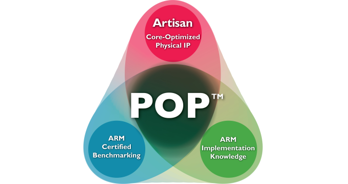
| 10:00a | ARM Announces 10FF "Artemis" Test Chip
Today in collaboration with TSMC, ARM's physical IP division is announcing the tapeout of a 10nm test chip demonstrating the company's readiness for the new manufacturing process. The new test chip is particularly interesting as it contains ARM's yet-to-be-announced "Artemis" CPU core. ARM discloses that tapeout actually took place back in December 2015 and is expecting silicon to come back from the foundry in the following weeks.
The test chip serves as a learning platform for both ARM and TSMC in tuning their tools and manufacturing process to achieve the best results in terms of performance, power, and area. ARM actually implemented a full 4-core Artemis cluster on the test chip which should serve as a representative implementation of what vendors are expected to use in their production designs. The test chip also harbours a current generation Mali GPU implementation with 1 shader core that serves as a demonstration of what vendors should expect when choosing ARM's POP IP in conjunction with its GPU IP. Besides the CPU and GPU we find also a range of other IP blocks and I/O interfaces that are used for validation of the new manufacturing process.
TSMC's 10FF manufacturing process primarily promises a large improvement in density with scalings of up to 2.1x compared to the previous 16nm manufacturing node. At the same time, the new process is able to achive 11-12% higher performance at each process' respective nominal voltage, or a 30% reduction in power at the same frequency.
In terms of a direct comparison between a current Cortex A72 design on 16FF+ and an Artemis core on 10FF on the preliminary test chip with an early physical design kit (PDK) we see that the new CPU and process are able to roughly halve the dynamic power consumption. Currently clock frequencies on the new design still don't reach what is achievable on the older more mature process and IP, but ARM expects this to change in the future as it continues to optimise its POP and the process stabilises.
As manufacturing processes increasingly rise in their complexity, physical design implementation becomes an increasingly important part of CPU and SoC designs. As such, tools such as ARM's POP IP become increasingly important for vendors to be able to achieve a competitive result both in terms of PPA and time-to-market of an SoC. Today's announcement serves as demonstration of ARM commitment to stay ahead of the curve in terms of enabling its partners to make the best out of the IP that they license. | ||||||||||||||||||||||||||||||||||||||||||||||||||||||||||||||||||||||||||||||||||||||||||||
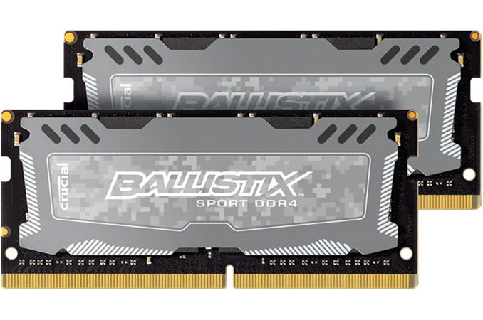
| 11:45a | Crucial Announces 16GB Ballistix Sport LT DDR4-2400 SO-DIMMs
This week Crucial is introducing its first DDR4 SO-DIMMs for enthusiasts, designed for high-performance notebooks and small form-factor PCs. The Crucial Ballistix Sport LT PC4-19200 SO-DIMMs are available in 4 GB, 8 GB and 16 GB capacities and can operate at DDR4-2400 with 16 16-16 timings with 1.2 volts. The modules feature SPD with XMP 2.0 profiles for devices that support XMP. PC makers focusing on Intel enthusiast mobile parts usually ship their computers with DDR4-2133 memory modules, as per the JEDEC standard and the supported standard on the chips, and provides a peak 34.1 GB/s bandwidth when operating in dual-channel mode. By contrast, a pair of DDR4-2400 SO-DIMMs enables 38.4 GB/s of bandwidth, or 12.6% higher, which could provide a noteworthy performance improvement in applications that demand memory bandwidth (e.g., graphics applications). At the same time, the binned 2400 MT/s data rate and 1.2 volts modules with additional heatsinks are geared to maintain temperature equilibrium similar to the base frequency modules. In short, it should be relatively safe to use such modules even in highly-integrated systems with moderate cooling.
The prices of the dual module kits are slightly above buying two single modules, but that's for good reason: users who want more than one module and want guaranteed system compatibility between modules should buy a complete kit. This is because tertiary sub-timings on a multi-module kit are adjusted to compensate for having more than one module (or rather, a kit with fewer modules has tighter timings as it doesn't have as many modules to compensate for). When a user buys individual modules (or a couple of two-module kits rather than a four-module kit), there's no guarantee the memory will work together. Many users might not have issues putting modules together because there's enough wiggle room in the memory controller or the ICs to compensate, but plenty of problems can arise from this, especially when moving to faster speed kits. AnandTech has historically always recommended buying a full multi-module kit with the required capacity in one go, over buying separate modules/mini-kits over time. The Ballistix Sport LT DDR4 SO-DIMMs will be available for purchase globally from retailers shortly and are currently available from the Crucial website. The modules are backed by a limited lifetime warranty (except Germany, where the warranty is valid for 10 years from the date of purchase). | ||||||||||||||||||||||||||||||||||||||||||||||||||||||||||||||||||||||||||||||||||||||||||||
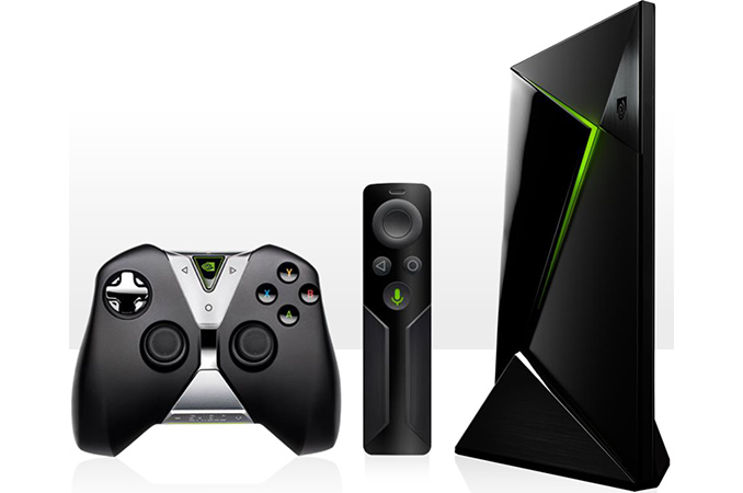
| 6:00p | NVIDIA SHIELD Android TV Console Adds Support for Vudu, HDR and 4Kp60 Content
The NVIDIA SHIELD Android TV set-top-box continues to be the most advanced device featuring Google’s TV platform even a year after it was introduced into the market. The credit goes mainly to the high-end Tegra X1 SoC as well as the rich feature-set that has been getting continuous updates from NVIDIA. Today, the company is announcing several important improvements to the unit, including support for HDR as well as 4Kp60 playback. The NVIDIA SHIELD Android TV has rather rich gaming capabilities. It supports a library of Android games compatible with its gamepad. It also supports GameStream technology, which allows for games to be streamed from a suitably equipped GeForce GTX PC. Besides, it supports the GeForce Now subscription service, which can stream new games rendered in NVIDIA’s datacenters to the console. In addition to games, NVIDIA has also been serious about enabling access to other types of content, including movies, music, sports and news.
At its launch a year ago, the NVIDIA SHIELD Android TV supported various video streaming services. The most popular among them included Netflix, YouTube, Hulu Plus and Vevo. However, certain services such as Vudu were notably absent. At the Google I/O conference today, NVIDIA announced that its upcoming Upgrade 3.2 for the SHIELD Android TV will bring support for new content providers, including ABC, Vudu, Spotify, MTV and Disney.
The Vudu content delivery application for Google’s Android TV will support streaming of ultra-high-definition 4K movies, adding another option for premium TV owners. In addition to UHD video, Vudu promises to support Dolby Atmos surround sound audio. Dolby Atmos is a nice addition to SHIELD’s lossless audio support. The Vudu Android TV app will be an exclusive on the SHIELD Android TV for some time to come. Owners of the device will be able to acquire 4K content from more than six providers, including Netflix, Hulu, HBO Go, Vudu, Plex, UltraFlix and Curiosity Stream. While Vudu is a new addition to the NVIDIA SHIELD Android TV, the Netflix app is also receiving improvements. With Upgrade 3.2, SHIELD Android TV owners can now play back select 4K titles with HDR (high dynamic range). From a technical standpoint, HDR-mastered 4K video streams contain special metadata flags that help HDMI 2.0a-supporting hardware to display scenes with 10-bit color depth and a greater color gamut properly. We already saw in our review that Netflix streams HEVC 10-bit video for some of the 4K titles, though all 10-bit videos are not necessarily HDR-enabled.
HDR support will not be limited only to Netflix. NVIDIA also plans to add HDR streaming to its GameStream technology later this summer. Encoding of HDR-enabled streams will only be available on GeForce GTX graphics cards based on the company’s latest Pascal architecture. This is not really surprising as the GP104 is currently the only GPU in NVIDIA’s arsenal with the hardware-accelerated 10b encoding necessary for HDR with good quality.
Although the SHIELD Android TV was the industry’s first Android TV STB capable of decoding and displaying 4Kp60 (3840x2160 resolution at 60 fps) content, users were limited to local content in order to experience it. This will be changing shortly, as YouTube will soon make 4Kp60 content available on the STB. While NVIDIA has not revealed everything that is set to come to the SHIELD Android TV in the next few months, it did confirm that the STB will definitely get an upgrade to the next-generation Android N. The future Android TV operating system will support features such as live TV recording, picture-in-picture and so on. Given the fact that NVIDIA has been updating its SHIELD set-top-box regularly in the past year, it is likely that the company will upgrade it to the new Android TV version once the latter is released.
While NVIDIA is making the SHIELD Android TV better for existing users, the company is also working to expand its customer base. For a limited time only, it will bundle the SHIELD Remote ($49.99) for free along with the SHIELD 16 GB ($199.99) and the SHIELD Pro 500 GB ($299.99) set-top-boxes. | ||||||||||||||||||||||||||||||||||||||||||||||||||||||||||||||||||||||||||||||||||||||||||||
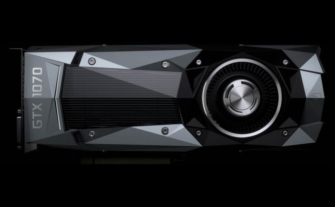
| 10:15p | NVIDIA Posts Full GeForce GTX 1070 Specifications: 1920 CUDA Cores Boosting to 1.68GHz
Back when NVIDIA first announced the GeForce GTX 1080 earlier this month, they also briefly announced that the GTX 1070 would be following it. The GTX 1070 would follow the GTX 1080 by two weeks, and presumably to keep attention focused on the GTX 1080 at first, NVIDIA did not initially reveal the full specifications for the card. Now with the GTX 1080 performance embargo behind them – though cards don’t go on sale for another week and a half – NVIDIA has posted the full GTX 1070 specifications over on GeForce.com.
Previously disclosed at 6.5 TFLOPs of compute performance, we now know how NVIDIA is getting there. 15 of 20 SMs will be enabled on this part, representing 1920 CUDA cores. Clockspeeds are also slightly lower than GTX 1080, coming in at 1506MHz for the base clock and 1683MHz for the boost clock. Overall this puts GTX 1070’s rated shader/texture/geometry performance at 73% that of GTX 1080’s, and is a bit wider of a gap than it was for the comparable GTX 900 series cards. However on the memory and ROP side of matters, the two cards will be much closer. The GTX 1070 is not shipping with any ROPs or memory controller channels disabled – GTX 970 style or otherwise – and as a result it retains GP104’s full 64 ROP backend. Overall memory bandwidth is 20% lower, however, as the GDDR5X of GTX 1080 has been replaced with standard GDDR5. Interestingly though, NVIDIA is using 8Gbps GDDR5 here, a first for any video card. This does keep the gap lower than it otherwise would have been had they used more common memory speeds (e.g. 7Gbps) so it will be interesting to see how well 8Gbps GDDR5 can keep up with the cut-down GTX 1070. 64 ROPs may find it hard to be fed, but there will also be less pressure being put on the memory subsystem by the SMs.
Meanwhile as is usually the case for x70 cards, GTX 1070 will have a lower power draw than its fully enabled sibling, with a shipping TDP of 150W. Notably, the difference between the GTX 1080 and GTX 1070 is larger than it was for the 900 series – where it was 20W – so we’re going to have to see if GTX 1070 ends up being TDP limited more often than GTX 1080 is. In that sense TDP is somewhat arbitrary – its purpose is to set a maximum power consumption for cooling and power delivery purposes – and I’m not surprised that NVIDIA wants to stay at 150W or less for the x70 series after the success that was the GTX 970. Like the GTX 1080, the GTX 1070 will be launching in two configurations. The base configuration is starts at $379 and will feature (semi) custom partner designs. Meanwhile as previously disclosed, NVIDIA will be offering a Founders Edition version of this card as well. The Founders Edition card will be priced at $449 – a $70 premium – and will be available on day one, whereas this is not guaranteed to be the case for custom cards. The GTX 1070 Founders Edition card will retain the basic stylings of the GTX 1080, including NVIDIA’s new angular shroud. However I have received confirmation that as this is a lower TDP card, it will not get the GTX 1080’s vapor chamber cooler. Instead it will use an integrated heatpipe cooler similar to what the reference GTX 980 used. | ||||||||||||||||||||||||||||||||||||||||||||||||||||||||||||||||||||||||||||||||||||||||||||


| << Previous Day |
2016/05/18 [Calendar] |
Next Day >> |