[Most Recent Entries] [Calendar View]
Monday, August 1st, 2016
| Time | Event | ||||||||||||||||||||||||||
| 5:00a | Hidden Secrets: Investigation Shows That NVIDIA GPUs Implement Tile Based Rasterization for Greater Efficiency
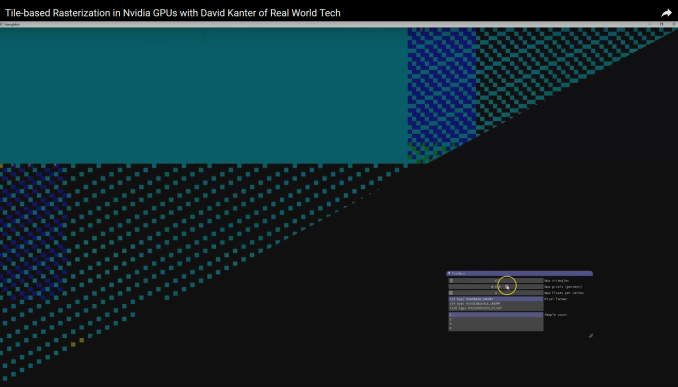
As someone who analyzes GPUs for a living, one of the more vexing things in my life has been NVIDIA’s Maxwell architecture. The company’s 28nm refresh offered a huge performance-per-watt increase for only a modest die size increase, essentially allowing NVIDIA to offer a full generation’s performance improvement without a corresponding manufacturing improvement. We’ve had architectural updates on the same node before, but never anything quite like Maxwell. The vexing aspect to me has been that while NVIDIA shared some details about how they improved Maxwell’s efficiency over Kepler, they have never disclosed all of the major improvements under the hood. We know, for example, that Maxwell implemented a significantly altered SM structure that was easier to reach peak utilization on, and thanks to its partitioning wasted much less power on interconnects. We also know that NVIDIA significantly increased the L2 cache size and did a number of low-level (transistor level) optimizations to the design. But NVIDIA has also held back information – the technical advantages that are their secret sauce – so I’ve never had a complete picture of how Maxwell compares to Kepler. For a while now, a number of people have suspected that one of the ingredients of that secret sauce was that NVIDIA had applied some mobile power efficiency technologies to Maxwell. It was, after all, their original mobile-first GPU architecture, and now we have some data to back that up. Friend of AnandTech and all around tech guru David Kanter of Real World Tech has gone digging through Maxwell/Pascal, and in an article & video published this morning, he outlines how he has uncovered very convincing evidence that NVIDIA implemented a tile based rendering system with Maxwell. In short, by playing around with some DirectX code specifically designed to look at triangle rasterization, he has come up with some solid evidence that NVIDIA’s handling of tringles has significantly changed since Kepler, and that their current method of triangle handling is consistent with a tile based renderer.
Tile based rendering is something we’ve seen for some time in the mobile space, with both Imagination PowerVR and ARM Mali implementing it. The significance of tiling is that by splitting a scene up into tiles, tiles can be rasterized piece by piece by the GPU almost entirely on die, as opposed to the more memory (and power) intensive process of rasterizing the entire frame at once via immediate mode rendering. The trade-off with tiling, and why it’s a bit surprising to see it here, is that the PC legacy is immediate mode rendering, and this is still how most applications expect PC GPUs to work. So to implement tile based rasterization on Maxwell means that NVIDIA has found a practical means to overcome the drawbacks of the method and the potential compatibility issues. In any case, Real Word Tech’s article goes into greater detail about what’s going on, so I won’t spoil it further. But with this information in hand, we now have a more complete picture of how Maxwell (and Pascal) work, and consequently how NVIDIA was able to improve over Kepler by so much. Finally, at this point in time Real World Tech believes that NVIDIA is the only PC GPU manufacturer to use tile based rasterization, which also helps to explain some of NVIDIA’s current advantages over Intel’s and AMD’s GPU architectures, and gives us an idea of what we may see them do in the future. | ||||||||||||||||||||||||||
| 9:00a | The Alphacool Eisbaer 240 CPU AIO Liquid Cooler Review Alphacool has been a known manufacturer of liquid cooling products for many years but had virtually no presence in the mainstream market until recently. In this review we are having a look at the company’s first AIO liquid cooling CPU cooler, the Eisbaer. This is a product targeted at a wide audience of users, but that also faces a lot of competition from numerous other products. | ||||||||||||||||||||||||||
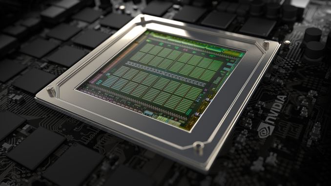
| 10:00a | SK Hynix Adds HBM2 to Catalog: 4 GB Stacks Set to Be Available in Q3
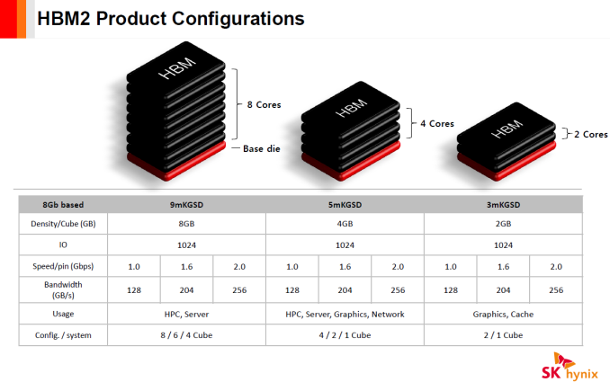
SK Hynix has quietly added its HBM Gen 2 memory stacks to its public product catalog earlier this month, which means that the start of mass production should be imminent. The company will first offer two types of new memory modules with the same capacity, but different transfer-rates, targeting graphics cards, HPC accelerators and other applications. Over time, the HBM2 family will get broader. SK Hynix intends to initially offer its clients 4 GB HBM2 4Hi stack KGSDs (known good stack dies) based on 8 Gb DRAM devices. The memory devices will feature a 1024-bit bus as well as 1.6 GT/s (H5VR32ESM4H-12C) and 2.0 GT/s (H5VR32ESM4H-20C) data-rates, thus offering 204 GB/s and 256 GB/s peak bandwidth per stack. Earlier this year a representative for SK Hynix revealed plans (in an interview with Golem.de) to start volume production of 4 GB HBM2 KGSDs in Q3 and the addition of the devices into product catalog confirms this information. Keep in mind that memory companies usually make announcements about the start of mass production when they are ready to deliver the first batch of new DRAM to a customer(s). Therefore, it is possible that SK Hynix may already be producing HBM2 stacks.
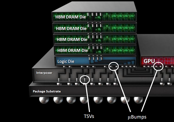
As outlined in our article published earlier this year, HBM2 memory can stack two, four or eight DRAM devices (2Hi, 4Hi, 8Hi stacks) interconnected using through silicon vias (TSVs) on a base logic die per KGSD (known good stacked die). Each DRAM device features two 128-bit channels, which use DDR signaling with a 2n prefetch architecture (256 bits per memory read and write access) and can operate at their own frequency or even in their own mode. SK Hynix uses 21 nm process technology to make its HBM2 memory and eventually plans to offer 2 GB and 8 GB KGSDs (featuring two or eight 8 Gb DRAM ICs) in addition to 4 GB stacks, aimed at providing memory for various applications. All HBM2 memory products from the company will have 1.2 V VDD/VDDQ and will come in new packages featuring 7.75 mm × 11.87 mm (91.99 mm2) dimensions. Samsung Electronics began to mass produce its 4 GB 4Hi stack HBM2 KGSDs featuring 2 GT/s data-rate earlier this year and NVIDIA employed the new chips for its GP100 GPU. The first NVIDIA-branded card to use the HBM2 is the Tesla P100 compute accelerator, which has 16 GB of HBM2 memory with 720 GB/s bandwidth (as the DRAM interface operates at about 1.4 GT/s data-rate).
Speaking of HBM2 usage by commercial SoCs, last year SK Hynix said that it worked with 10 companies on various projects (including ASICs, x86 processors, ASSPs and FPGAs) featuring HBM memory (both generations), which indicates that the interest for multi-layer high-bandwidth DRAM is here. However, so far only AMD and NVIDIA have introduced actual products featuring HBM and HBM2. When it comes to the original HBM, it is worth to mention that SK Hynix has removed such stacks from its catalog. It is unknown whether the company continues to ship them to interested parties, but given the fact that there are not a lot of products that utilize HBM1 today, small scale shipments should not be a problem (at least, until SK Hynix phases out its 29 nm production lines). Meanwhile, since HBM2 is here, it is feasible to assume that we are not going to see many new devices utilizing HBM1. | ||||||||||||||||||||||||||
| << Previous Day |
2016/08/01 [Calendar] |
Next Day >> |