[Most Recent Entries] [Calendar View]
Friday, August 12th, 2016
| Time | Event | ||||||||||||||||||||||||||||||||||||||||||||
| 8:00a | Western Digital to Use 3D ReRAM as Storage Class Memory for Special-Purpose SSDs
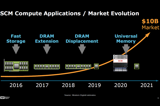
At the Flash Memory Summit this week, Western Digital announced that it intends to use 3D Resistive RAM (ReRAM) as storage class memory (SCM) for its future special-purpose ultra-fast SSDs. The company did not reveal any actual timelines for appropriate products, nor their specifications. However, what is important is the fact that Western Digital decided to use SanDisk’s long-discussed ReRAM along with 3D manufacturing tech to build the aforementioned special-purpose SSDs. The amount of data that the world produces totals several zettabytes per year, which creates two challenges for the high-tech industry: one is to store the vast amounts of data more or less cost-efficiently, another is to process this data efficiently from power consumption point of view. Modern SSDs and HDDs can store plenty of information (10 to 15 TB for top-of-the-range models) and modern CPUs can process a lot of data due to increasing number of cores. However, delivering the right data to those cores poses further challenges: if the necessary data is located on an HDD/SSD, fetching them from there takes a lot of time on computer timescales (e.g., 100,000 – 10,000,000 ns) and consumes a lot of energy. Meanwhile, increasing the amount of DRAM per server is not always feasible from economic point of view.
To address the challenge, the industry came up with idea of non-volatile SCM, which would sit between DRAM and storage devices and deliver much greater performance, endurance and lower latency (e.g., 250 – 5,000 ns) than NAND while costing a lot less than DRAM in terms of per-GB prices. Historically, different companies demonstrated various types of memory, which could be used as SCM (originally, this class of devices was classified as a replacement tech for NAND flash), including conductive-bridging RAM (CBRAM), phase-change memory (PCM), magnetoresistive RAM (MRAM), resistive RAM (ReRAM) and some others. All of these technologies have their own peculiarities like performance and costs (and none of them could beat NAND in terms of per-GB cost), but SanDisk has been working for years on bringing ReRAM to the market.
Fundamentally, ReRAM (also sometimes called RRAM) works by changing the resistance across a dielectric material by electrical current (which is why 3D XPoint is considered as a proprietary implementation of ReRAM). The resistance can be measured and considered as “0” or “1”. On paper, the technology enables higher performance and endurance when compared to NAND flash, but finding the right materials and architecture for ReRAM has taken engineers many years.
Without making any significant announcements this week, Western Digital indicated that it would use some of the things it has learnt while developing its BiCS 3D NAND to produce its ReRAM chips. The company claims that its ReRAM will feature a multi-layer cross-point implementation, something it originally revealed a while ago.
Perhaps, the most important announcement regarding the 3D ReRAM by Western Digital is the claim about scale and capital efficiency of the new memory. Essentially, this could mean that the company plans to use its manufacturing capacities as well as its infrastructure (testing, packaging, etc.) in Yokkaichi, Japan, to make 3D ReRAM. Remember that SCM is at this point more expensive than NAND, hence, it makes sense to continue using the current fabs and equipment to build both types of non-volatile memory so ensure that the SCM part of the business remains profitable. IMFT does the same thing with its SCM: it uses its fab in Lehi, Utah, to produce 3D XPoint memory, but does not reveal specifics about the process technology (just like Western Digital). Of course, Western Digital could re-use some of the fundamental technologies, materials and process architecture both for ReRAM and NAND, but the company does not any particular details on the matter just now.
Quite naturally, WD’s 3D ReRAM will scale in terms of per-IC densities with the increase of the number of layers, though, we do not know how many layers will initial 3D ReRAM ICs from Western Digital incorporate. However, the company seems to be very optimistic about scaling of its SCM and believes that over time it will close the gap in terms of per-GB cost with BiCS NAND and will thus widen the gap with DRAM, which will make it more economically feasible.
Finally, the manufacturer said that its 3D ReRAM is already supported by the ecosystem, which means that the first SSDs based on the technology will probably use industry-standard interfaces (e.g. NVDIMM), which is not surprising. Perhaps, it also means that Western Digital is also already working with software developers to ensure that applications can take advantage of SCM in general, but we cannot confirm this at this time. To sum up, Western Digital has finished development of ReRAM, which SanDisk has been discussing for several years now. The company plans to release actual products based on ReRAM in the foreseeable future (12 – 24 months from now, call it a guess) and to use the same fab and equipment to build ReRAM and NAND ICs. Western Digital’s ReRAM has a roadmap for the future. What remains to be seen is what is going to happen to the joint development of SCM announced by SanDisk and HP in October, 2016. | ||||||||||||||||||||||||||||||||||||||||||||
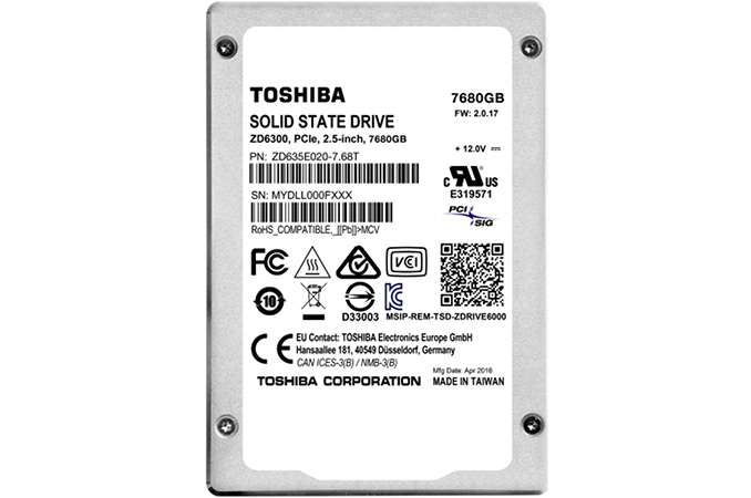
| 2:00p | Toshiba Begins to Sample eMLC-Based ZD6300 7.68 TB SSDs to Customers
Toshiba has quietly expanded its ZD6300 family of SSDs with a 7.68 TB model, its most capacious storage device announced to date. The new drive was designed for mixed workloads and uses Toshiba’s time-proven A19 eMLC NAND flash memory. Due to enhanced endurance and a lot of NAND used for overprovisioning, the SSD can be pre-ordered for approximately $12,000, depending on the seller, though its official MSRP is still unknown. The Toshiba ZD6300 7.68 TB (ZD635E020-7.68T) SSD uses PMC-Sierra’s “Princeton” controller (which is now called Flashtec NVMe PM8604 1032) with PCIe 3.0 x8 interface (which Toshiba splits into two x4 interfaces), 16 NAND flash channels and NVMe 1.1b protocol. The drive will be available in 2.5”/15 mm form-factor with U.2 connector (SFF-8639) in a bid to enable compatibility with different server chassis (specifically for those, which support multiple SSDs). The new 7.68 TB drive from Toshiba support the same functionality as other ZD-series drives from the company (which were originally introduced under OCZ brand), such as dual-port capability, AES-256 encryption, full power loss protection, end-to-end data protection and so on.
The ZD6300 7.68 TB SSD uses higher durability eMLC memory to guarantee better endurance, which is why it supports maximum sequential write speed of up to 2.9 GB/s (in line with the ZD6000-series drives). However its maximum sequential write speed is 1.4 GB/s (or actually lower) due to higher program latencies of eMLC (which is in line with other ZD6300-series products). Typically, the key differences between the ZD6000 and the ZD6300 SSDs (which were officially announced) were usage of eMLC by the latter in order to enable three drive writes per day (DWPD) over a five-year period, which was more suitable for mixed workloads (something that the ZD6300 were designed for). What is important is that the Toshiba ZD6300 7.68 TB SSD belongs to the less-known Max Capacity sub-family from the Z-Drive 6300 product stack that uses eMLC, but not in order to enable 3 DWPDs, but to maximize capacity using more durable ICs. The ZD6300 Max Capacity family has not been announced officially, but such SSDs are available for purchase (as pointed out by Ilya Gavrichenkov, my former colleague from another web-site). The ZD6300 Max Capacity drives do not reserve vast amounts of eMLC NAND flash for overprovisioning, unlike the regular ZD6300-series products, to enhance endurance, but this allows it to increase capacities by 20%, albeit at a relatively high per-gigabyte cost. Consequently, from a raw NAND capacity configuration point of view, Toshiba’s ZD6300 7.68 TB SSD is the same drive as the ZD6300 6.4 TB product: it has 8128 GB of memory, but it makes 7680 GB available to the user rather than 6400 GB. Just like the ZD6300 6.4 TB drives, the 7.68 TB model uses 32 of 16-die packages featuring 128 Gb eMLC NAND flash memory devices produced using Toshiba’s second-generation 19 nm process technology. It should be noted that apart from the ZD6000/ZD6300 SSDs with one or three DWPD, Toshiba also offers high-endurance SSDs with 10 or 25 DWPDs in their ZD-series product lineup. Such drives are naturally more expensive, but those, who need very high endurance, are usually willing to invest in such storage solutions. Still, since requirements of such customers are very diverse, Toshiba does not publish specs of such drives because virtually all of them are built to order and are not available from usual resellers.
Speaking of availability, Toshiba tells us that it is sampling the ZD6300 7.68 TB product with customers. Meanwhile, there are several resellers, who are offering to pre-order the SSD for $12,563, $12,090 or even $11,252. Since the product is still in the sampling stage and is not yet officially shipping, Toshiba naturally keeps its actual price under wraps. | ||||||||||||||||||||||||||||||||||||||||||||


| << Previous Day |
2016/08/12 [Calendar] |
Next Day >> |