[Most Recent Entries] [Calendar View]
Wednesday, August 17th, 2016
| Time | Event | |||||||||||||||||||||||||||||||||||||||||||||||||||||||||||||||||||||||||||||||||||||||
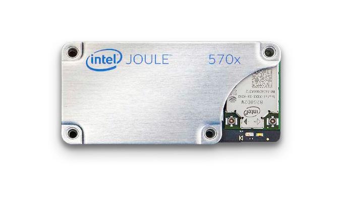
| 4:30a | Intel Unveils Joule: A High-Performance Atom-Powered IoT Module & Maker Kit
Today at Intel’s annual Developer Forum, the hardware manufacturer announced the latest in their Internet of Things-focused product kits: Joule. Based around Intel’s canceled-but-not-quite Broxton Atom processor, Joule is designed to further augment Intel’s existing lineup of kits by offering a much higher performance part based on the latest generations of the company’s technologies. Back in 2013 Intel announced Galileo, the first of what has become a collection of IoT kits/platforms for hardware developers. Galileo and its compatriots Edison and Curie turned out to be solid hits for the company – even with competing kits already on the market – driving a big part of Intel’s overall IoT growth in recent years. The System on Module boards proved popular with tinkers and product developers alike who needed small systems for everything from small prototypes to a commercial off the shelf boards.
Joule then extends Intel’s presence in this market by offering a higher performing part in their IoT portfolio. Whereas the previous top-tier Edison board used a combination of Atom Silvermont and Quark CPU cores and paired this up with a respectable amount of RAM, NAND, and I/O options, Joule goes much further. The SoC at the heart of the board is Intel’s Broxton-M, which although was canceled for consumer devices, as we can now see will instead be making a home for itself within Intel’s IoT product family. Intel is offering two different versions of the Joule board. Both use the same SoC, but they vary in clockspeeds and memory. The more powerful of the two, Joule 570X, uses what Intel is calling a Atom T5700, which is a quad core Goldmont Atom configuration with a base clock of 1.7GHz and can turbo to 2.4GHz. This in turn is paired with 4GB of LPDDR4 memory and a 16GB eMMC NAND module for non-volatile storage. Meanwhile the Joule 550X drops the quad core Atom to 1.5GHz with no turbo, and features 3GB of LPDDR4 memory along with 8GB of NAND. Both Joule boards also feature the same I/O connectivity. On the wireless side, this is composed of a radio supporting Bluetooth 4.1 and 802.11ac (MIMO is listed supported, so I’m wagering this is a 2 spatial stream solution). And on the wired side, USB 3.0 is supported, along with the vast collection of GPIOs, UARTs, and MPI’s camera (CSI) and display (DSI) interfaces. The Joule module itself is said to only be a bit larger than the Edison module – which was usually measured relative to a postage stamp – and in the brief glimpse of the module we got when Brian Krzanich held it out on stage, I’d say we’re looking at something not too much bigger than a stick of gum (or perhaps the old Sony memory stick). Intel hasn’t released the full documentation for the kit yet, so we don’t have power consumption information available, but given the higher performance goals for the kit (and the quad Goldmont CPU cores), it’s a fair bet that it’s going to be higher than Edison.
As you might expect from the specifications, Intel is aiming Joule at a higher performance class of use cases. Ultimately as a maker kit it’s a bit of an “if you build it” situation – it’s up to developers to figure out what to do with it – but Intel sees it as being useful for drones, AR/VR, robotics, and for the first time in one of their IoT products, computer vision. While we don’t have a ton of hard details on the underlying iGPU, it is powerful enough for certain CV tasks, and it supports both 4K video capture and display. It also supports Intel’s RealSense camera, giving developers the option of using the underlying depth sensing capabilities for improved vision/analysis.
Finally, on the software side of matters, the Joule will support a few different OSes. The boards will default to a new Linux distribution specifically designed for the hardware that Intel is calling Reference Linux OS for IoT, and Cannonical’s “Snappy” Ubuntu Core is also supported. Meanwhile Microsoft’s Windows 10 IoT Core is also supported for developers who need Windows interoperability. Wrapping things up, along with today’s announcement, Intel has already begun selling one of the Joule SKUs, with the others to follow. The Joule 570X development kit, which includes the Joule module, carrier board, WiFi antennas, and other components is on sale today at IDF for $369, and will be available through Intel’s partners next month. At that price it’s fair to say that Intel is not aiming to have Joule compete with more mainstream kits – or even their own Edison kit – but rather at the more upscale kits such as the (even more expensive) NVIDIA Jetson TX1, which is a much tighter market in terms of the number of competitors. Meanwhile the lower-end 550X development kit and the stand-alone Joule modules are scheduled for release in Q4. Pricing for those products has not yet been disclosed, though given the intent for Joule to be used in mass production devices, it’ll be interesting to see what Intel prices the stand-alone modules at. | |||||||||||||||||||||||||||||||||||||||||||||||||||||||||||||||||||||||||||||||||||||||
| 5:20p | Intel Announces Knights Mill: A Xeon Phi For Deep Learning
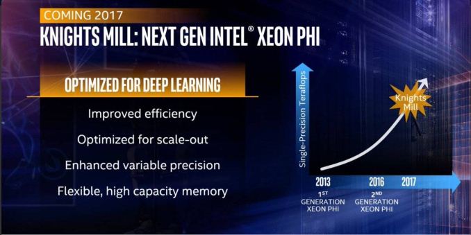
In a brief announcement as part of today’s Day 2 ketnote for IDF 2016, Intel has announced a new member of the Xeon Phi family. The new part, currently under the codename of Knights Mill, is being aimed at the deep learning market and is scheduled for release in 2017. At this point there are more unknowns than knowns about Knights Mill, in part because Intel has not offered much detail on how it fits into the larger Xeon Phi brand. The company had previously announced in 2014 that the successor to the current Knights Landing design would be Knights Hill, a true 3rd gen Xeon Phi built on Intel’s 10nm process. However this week there has been no mention of Knights Hill, whether Knights Mill is Knights Hill renamed, or what the manufacturing process Knights Mill is being made on. With that said, as Knights Mill is scheduled for 2017, it’s unlikely that it’s Knights Hill (at least as initially planned), as 2017 would be too early for a very large 10nm chip from Intel’s fabs.
Working on the assumption at the moment that Knights Mill is in fact its own part, what we do know is that with it, Intel is making a very clear play for the rapidly growing machine learning market, and indeed this will be its defining characteristic. Among the features/design tweaks for the new processor, Intel is adding what they are calling “variable precision” support. What that fully entails isn’t clear, but the use of lower precision modes has been a major factor in the development and subsequent high performance of machine learning-focused processors, so it’s likely that this means that Intel is adding FP16 and possibly other lower-precision modes, something the current Knights Landing lacks. As machine learning typically does not require high precision, these lower precision modes potentially allow for a major increase in processor throughput, as more, narrower operations can be packed into a SIMD. Also on the feature list is improved scale-out performance. It’s not clear right now if this is some kind of fabric/interconnect change, or if Intel has something else in mind. But the ultimate goal is to make clusters of Xeon Phi processors perform better, which is an important factor in bringing down the training time of very large and complex datasets. Meanwhile there are also unspecified memory changes for Knights Mill, with Intel touting the chip’s “flexible, high capacity memory.” Competitively, this is a shot across the bow at NVIDIA’s own Tesla products, and in their comments here at IDF and in previous presentations, Intel has not shied away from comparing their tech to GPUs and touting why they believe Xeon Phi to be superior. One such example, though briefly mentioned, is that like Knights Landing, Knights Mill is capable of acting as a host processor. So expect to see Intel promoting the benefits of not needing separate host processors & co-processors, and how Knights Mill can be attached directly to system RAM. This, along with the performance differences between the GPU architectures and Knights Mill, will undoubtedly be a recurring fight between the two companies both now and next year when the new processor actually launches. In the meantime, we’ll keep digging for more information on Knights Mill, and hopefully get a better idea of how it fits into the Xeon Phi family. (Image Courtesy The Register) | |||||||||||||||||||||||||||||||||||||||||||||||||||||||||||||||||||||||||||||||||||||||
| 7:30p | Marvell Announces NVMe Controller for DRAM-Less PCIe 3.0 x2 SSDs
Marvell has announced its new controller for affordable and miniature SSDs, the 88NV1160. The chip can be used to build small form-factor SSDs in M.2 as well as BGA packages. The 88NV1160 supports all modern and upcoming types of NAND flash, LDPC error correction, NVMe protocol and other advantages of modern SSD controllers, but it does not require external DRAM buffers so to reduce BOM costs of upcoming SSDs. The Marvell 88NV1160 is a quad-channel controller that supports PCIe 3.0 x2 interface, NVMe 1.3 protocol (in addition to AHCI) as well as various types of NAND flash memory, including 15 nm TLC, 3D TLC as well as 3D QLC with ONFI 3.0 interface with up to 400 MT/s transfer rates. The 88NV1160 controller is powered by dual-core ARM Cortex-R5 CPUs along with embedded SRAM with hardware accelerators to optimize IOPS performance. The chip supports Marvell’s third-generation LDPC error correction technology (which the company calls NANDEdge ECC) in a bid to enable high endurance of drives featuring ultra-thin TLC or 3D QLC memory.
The 88NV1160 controller is specifically tailored for upcoming affordable SSDs, which is why it does not officially support SLC and 2D MLC NAND. Maximum capacity of a 3D QLC-based SSD featuring the 88NV1160 controller is expected to be around 1 TB, which should be enough for entry-level SSDs (as well as solid-state storage solutions for premium tablets, ultrabooks and other types of computing devices). As for performance, Marvell mentioned 1600 MB/s maximum read speed for such SSDs. The new chip from Marvell is made using 28 nm process technology and is shipped in 9 × 10 mm TFBGA package, which can be used to build SSDs in BGA (M.2-1620 and smaller) packages as well as drives in M.2-2230/2242 form-factors. The 88NV1160 controller uses 3.3V/1.8V/1.2V power supply, in accordance with the M.2 standards. The 88NV1160 is not the first controller from Marvell that does not require any external DRAM buffers. The company also offers low-cost 88NV1120 with SATA interface as well as 88NV1140 for PCIe 3.0 x1 SSDs. All of the aforementioned controllers are based on two ARM Cortex-R5 cores, feature Marvell’s third-gen LDPC implementation and support modern types of NAND flash memory (15nm 2D TLC and 3D TLC/QLC). However, the new 88NV1160 is the newest DRAM-less controller from the company, which is designed for rather advanced SSDs with up to 1600 MB/s read speed. Still, the 88NV1160 is clearly a solution for affordable drives because unlike the high-end 88SS1093 (or its less advanced brother, the 88SS1094) it does not support 2D MLC and SLC NAND flash and cannot take advantage of eight NAND channels (which is why it does not need PCIe 3.0 x4).
The developer did not reveal when it expects the first SSDs based on the 88NV1160 controller to hit the market, but it indicated that the chip is available for sampling globally. In addition, the company indicated that it offers turnkey firmware to its customers so to enable faster time to market. | |||||||||||||||||||||||||||||||||||||||||||||||||||||||||||||||||||||||||||||||||||||||


| << Previous Day |
2016/08/17 [Calendar] |
Next Day >> |