[Most Recent Entries] [Calendar View]
Thursday, August 18th, 2016
| Time | Event | |||||||||||||||||||||||||||||||||||||||||||||||||||||||||||||||||||||||||||||||||||||||||||||||||||||||||||||||||||||||
| 7:00a | Micron Cancels Ballistix TX3 NVMe SSD
At Computex in June, Micron announced that Crucial's Ballistix brand was being promoted to a standalone brand for gaming-oriented products. Their exhibit included three tiers of Ballistix DRAM products and one SSD: the Ballistix TX3 M.2 PCIe SSD. Based on Micron 3D MLC NAND and the Silicon Motion SM2260 NVMe SSD controller, the TX3 was to be Micron's first consumer/retail SSD with 3D MLC or a PCIe interface and was slated for a release sometime in the second half of 2016.
Micron has informed us this week that the Ballistix TX3 program has been canceled. This leaves Micron's consumer SSD strategy up in the air. With the release this summer of the Crucial MX300, Micron moved their mainstream SATA MX line from MLC to 3D TLC NAND, casting doubt on the future of the value-oriented BX series and implying that their 3D MLC might be regarded as premium enough to be reserved for PCIe SSD. With the Ballistix TX3 canceled, we no longer have any clear indication of how Micron plans to move forward with their consumer SSD products. Micron may have decided to switch SSD controllers. While Silicon Motion reported last week at Flash Memory Summit that final firmware for the SM2260 controller is ready, Phison's E7 controller is also available and ready to roll out, and Micron has been shipping Marvell's 88SS1093 NVMe controller on their 7100 series enterprise SSDs in both U.2 and M.2 form factors, albeit with planar MLC NAND rather than their 3D NAND. Micron may also have decided that the timing was wrong to be getting into a market segment that Samsung has been handily dominating; beating Samsung's PCIe M.2 drives on performance will be an uphill battle to say the least, and substantially undercutting them on price may not be possible while Micron is still ramping up production of their 3D MLC NAND. Micron's OEM and enterprise offerings may offer some clues to their plans, but the Micron and Crucial SSD product lines are no longer mere alter egos of each other. Micron's 1100 series SATA SSD is the nearest equivalent to the MX300 with the same controller and same 3D TLC NAND, but the 1100 is more a little more conservative by retaining the traditional power of two drive capacities with generous overprovisioning while the MX300 dedicates some of the extra capacity of Micron's 3D TLC chips to increasing the usable drive capacity.
Micron announced a 2100 series at the same time as the 1100 series, but did not provide full details as it was scheduled for a later introduction than the 1100, but still by the end of summer this year. The photos provided of the 2100 clearly showed the Silicon Motion SM2260 controller and the drive was stated to be using 3D NAND, but whether it would be MLC or TLC was not specified. The layout of the 2100 M.2 card was different than that of the Ballistix TX3 prototypes shown at Computex, but they still clearly had a few things in common. Micron's website still lists the 2100 as "Coming Summer 2016", and with regards to its fate Micron had this statement for us:
We are eager to hear what Micron decides to do, as they are still only the second manufacturer to deliver 3D NAND for the client and consumer SSD market and we have not yet had the chance to test their 3D MLC NAND. Competition in the consumer PCIe SSD space will be heating up with or without Micron's participation as more drives based on Phison, Marvell and Silicon Motion PCIe NVMe controllers hit the market over the next few months, but Micron's entry was particularly promising for the inclusion of 3D NAND. | |||||||||||||||||||||||||||||||||||||||||||||||||||||||||||||||||||||||||||||||||||||||||||||||||||||||||||||||||||||||
| 7:00a | More Details on Broxton: Quad Core, ECC, Up to 18 EUs of Gen9
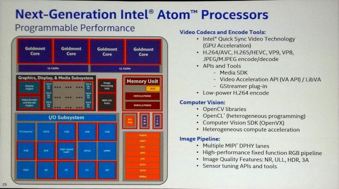
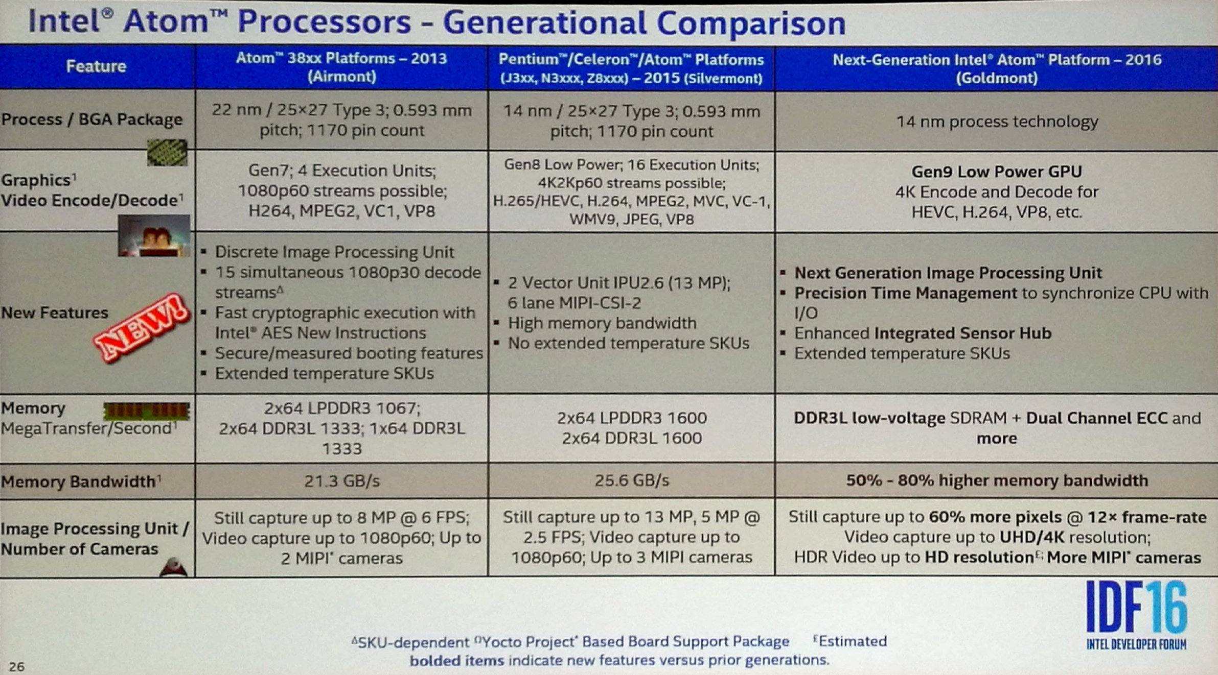
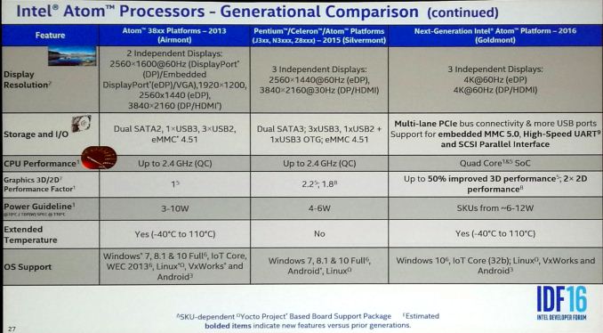
An interesting talk regarding the IoT aspects of Intel’s Next Generation Atom Core, Goldmont, and the Broxton SoCs for the market offered a good chunk of information regarding the implementations of the Broxton-M platform. Users may remember the Broxton name from the cancelled family of smartphone SoCs several months ago, but the core design and SoC integration is still mightily relevant for IoT and mini-PCs, as well as being at the heart of Intel’s new IoT platform based on Joule which was announced at IDF this week as well. Broxton in the form that was described to us will follow the previous Braswell platform in the sense that it runs in a quad-core configuration (for most SKUs) consisting of two sets of dual cores sharing a common L3 cache, but will be paired with Intel’s Gen9 graphics. The GPU configuration will be either in a 12 execution unit (EU) or 18 EU format, suggesting that the core will have a single graphics slice and will implement Intel’s binning strategy to determine which EUs are used on each sub-slice.
It was listed that Broxton will support VP9 encode and decode, as well as H.264. HEVC will be decode but they were hazy in clarifying decode support, saying that ‘currently we have a hybrid situation but this will change in the future’. There will also be OpenCV libraries available for Computer Vision type workloads to take advantage of optimized libraries that focus specifically on the graphics architecture.
It’s worth noting that on this next slide it notes the memory controller supporting DDR3L and LPDDR4, and later on in the presentation it only stated DDR3L. We asked about this, and were told that LPDDR4 was in the initial design specification, but may or may not be in a final product (or only in certain SKUs). However, DDR3L is guaranteed.
It was confirmed that Broxton is to be produced on Intel’s 14nm process, featuring a Gen9 GPU with 4K encode and decode support for HEVC (though not if this is hardware accelerated or hybrid or not). The graphics part will feature an upgraded image processing unit, which will be different to other Gen9 implementations, and we will see the return of extended temperature processors (-40C to 110C) for embedded applications. One of the big plus points for Broxton will be the support of dual channel ECC memory. This opens up a few more markets where ECC is a fundamental requirement to the operation. The slides also state a 50-80% higher memory bandwidth over Braswell, which is an interesting statement if the platform does not support LPDDR4 (or it’s a statement limited to the specific SKUs where LPDDR4 is supported).
All the displays from the Broxton SoC will support 4K60 outputs on eDP and DP/HDMI, along with more USB ports and support for eMMC 5.0. The support for 4K on HDMI might suggest full HDMI 2.0 support, however it is not clear if this is 4:2:0 chroma support or higher. The Broxton SKUs in this presentation were described as having a 6-12W TDP, with support on a number of Linux flavors, Android, and Windows 10. We asked about Windows 7 support, and we were told that while Broxton will likely support it, given the limited timeframe it is not expected to be promoted as a feature. We asked other questions on frequency, and were told to expect quad-core parts perhaps around 1.8-2.6 GHz. This would be in line with what we expect – a small bump over Braswell. We are still waiting on more detailed information regarding Goldmont and Goldmont-based SoCs like Broxton, and will likely have to wait until they enter the market before the full ecosystem of products is announced. | |||||||||||||||||||||||||||||||||||||||||||||||||||||||||||||||||||||||||||||||||||||||||||||||||||||||||||||||||||||||
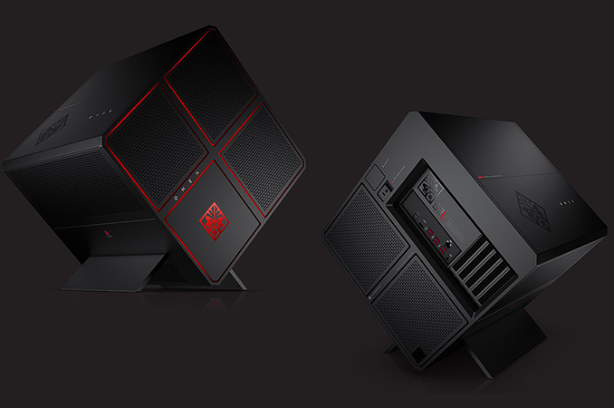
| 8:30a | HP and MAINGEAR Team Up for Omen X High-End Gaming PC
HP this week re-entered the market of high-end gaming PCs with its Omen X desktop. The machine uses rather unusual cube-shaped tri-chamber design featuring high-end hardware, liquid cooling and various upgrade options. HP will offer customized versions of the Omen X, but MAINGEAR will sell something more exclusive with additional customization options, Intel Core i7 Extreme CPUs, hand-build liquid cooling as well as factory overclocking. The year was 2006. PC gaming was not particularly on the rise (and the word eSports was non-existent), but the interest towards high-end PC gaming technologies was high, particularly because the demographics of gamers got older and more of those people could afford ultra-high-end gaming computers as well as components. This is when Dell acquired Alienware and HP bought Voodoo PC in a bid to address the growing and lucrative segment of the PC market. While the two large PC makers made a similar decision and bought leading boutique PC makers, there actions afterwards were substantially different. While both tried to integrate their gaming PC subsidiaries, Dell has succeeded and made Alienware its integral part of itself, whereas HP first ceased to sell expensive custom desktops, then started to place VoodooDNA brand on various high-end machines and then stopped building PCs for any demanding gamers at all. Apparently, HP was not interested in serving a relatively small segment of the PC market after multiple enterprise-oriented acquisitions. However, now that HP’s consumer business is a separate company, the latter seems to be gaining interest towards high-end machines, which is why it unveiled its Omen X system. Nonetheless, the company does not plan to address the market of boutique PCs just now, which is why it teamed up with MAINGEAR for advanced versions of the Omen X. While HP does not use the Voodoo brand for its Omen X, its machine carries the distinctive logotype on it.
The cube-shaped 45° angled design of the Omen X is meant to simplify access to hardware by the end-user. While the form of the Omen X is very distinctive, its concept is very similar to other modern desktops. The chassis sports three chambers to separate hot components (CPU+GPU, hard drives and PSU) from each other and optimally cool-down each chamber/set of components. The Omen X chassis can fit it one Micro-ATX motherboard (with one M.2 slot, two PCIe x16 slots, four DDR4 slots and so on), two graphics cards, two 3.5” storage devices/three 2.5” SSDs/HDDs, one M.2 SSD, one ODD, and one high-end PSU, with MAINGEAR offering up to a 1200 W Corsair AX1200i model.
While architecturally the HP Omen X and the MAINGEAR Omen X are exactly the same, there are substantial differences when it comes to their configurations, which is why we basically talking about two rather different systems here. HP only offers Intel’s LGA1151 processors as well as up to two AMD Radeon R9 Fury X or NVIDIA GeForce GTX 1080 graphics cards with its Omen X. By contrast, MAINGEAR offers only LGA2011-3 platforms, up to ten-core Core i7-6950X CPU, up to two NVIDIA Titan X (Pascal) graphics cards, hand-made liquid cooling as well as custom exterior finish with automotive paint. The differences of configurations naturally affect prices: the HP Omen X starts at $1800, whereas MAINGEAR-built Omen X starts at $3000 with more advanced “superstock” version available for $5200.
All Omen X systems use industry-standard components, so it will be possible for owners to upgrade them as they wish (subject to terms and conditions of warranty) using any aftermarket part. Still, keeping in mind that MAINGEAR offers custom liquid cooling solutions, it may not be that easy to upgrade such machines without re-building the LCS.
HP plans to start shipments of its Omen X at a later date, whereas MAINGEAR intends to ship its Omen X in mid-September. In addition to Omen X desktops, HP also plans to offer a complimentary set of Omen-branded peripherals (with Voodoo logotype on them). The initial family will include a headset and a mouse designed by SteelSeries as well as a 32” display. | |||||||||||||||||||||||||||||||||||||||||||||||||||||||||||||||||||||||||||||||||||||||||||||||||||||||||||||||||||||||
| 9:00a | AMD Zen Microarchitecture: Dual Schedulers, Micro-Op Cache and Memory Hierarchy Revealed In their own side event this week, AMD invited select members of the press and analysts to come and discuss the next layer of Zen details. In this piece, we’re discussing the microarchitecture announcements that were made, as well as a look to see how this compares to previous generations of AMD core designs. | |||||||||||||||||||||||||||||||||||||||||||||||||||||||||||||||||||||||||||||||||||||||||||||||||||||||||||||||||||||||
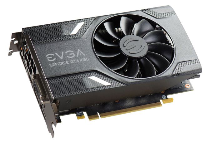
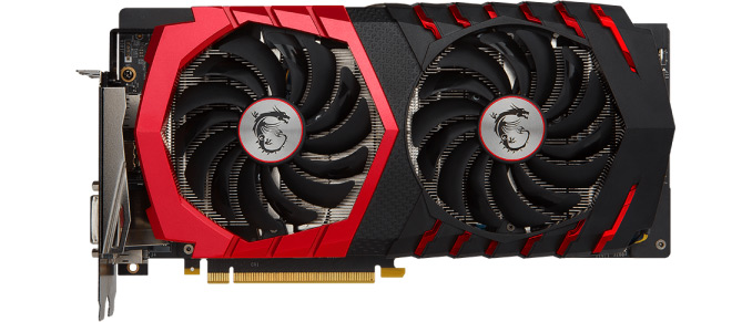
| 6:15p | NVIDIA Releases GeForce GTX 1060 3GB: GTX 1060, Yet Not
In a low-key press blast sent today, NVIDIA has announced that they are expanding the GeForce 10-Series of cards with another entry. Augmenting the current series of cards is a second GeForce GTX 1060, the GeForce GTX 1060 3GB, which despite the name is not actually equal to the original, 6GB GeForce GTX 1060. The new GTX 1060 3GB is available immediately from retailers starting at $199.
Looking at the big picture, the new GTX 1060 3GB materially differs from the existing 6GB GTX 1060 in two different metrics. First and foremost of course is the memory; the card ships with half as much memory, which amounts to a 6x512MB configuration. However, somewhat frustratingly, NVIDIA didn’t just stop there and has also introduced a new GPU configuration for this card, meaning that we are now looking at multiple GPU configurations being sold at retail under the GTX 1060 banner.
Whereas the original GTX 1060 6GB shipped with a fully enabled GP106 GPU, the GPU used in the GTX 1060 3GB ships with 1 of the 10 SMs disabled. This leaves 9 SMs enabled, leading to a CUDA core count of 1152, and 72 texture units. Other than this sole disabled SM, the GPU is otherwise untouched, and the full ROP/L2 backend and its associated memory controllers are fully enabled. Clockspeeds are also unchanged. On the GPU this means we’re still looking at 1506MHz base and 1709MHz boost. Meanwhile on the memory it’s still 8Gbps GDDR5 on a 192-bit memory bus, only now there’s only half as much total memory. Consequently the total performance hit to the GTX 1060 3GB as compared to the original GTX 1060 6GB will be a combination of the reduced memory capacity and the loss of 10% of the shading/texturing/geometry resources. Finally, on the TDP side, TDP hasn’t been adjusted even with the loss of 1 SM. This means TDP remains at 120W. I suspect part of this comes down to the fact that NVIDIA isn’t doing additional power binning (ala GTX 1070), along with the fact that disabling a single SM is going to have a limited impact on power consumption. All told, this is a typical case of NVIDIA creating a new SKU for salvaged GPUs. Since the full-fledged GTX 1060 uses an equally full-fledged GP106, this gives salvaged GP106s a card to use them in. The concern I have is that, frankly, I thought NVIDIA was done with these shenanigans, as they haven’t had multiple GPU configurations selling under a single retail GTX model number for a number of years now. To the company’s credit, they are drawing a clear line between the 3GB and 6GB cards – there will not be any 6GB cards with a cut-down GPU, nor any 3GB cards with the full GPU – but the memory configuration now means something about how the GPU is configured, which is unintuitive at best (ed: and this doesn’t give AMD a free pass on the RX 480 either). Ultimately I’m not sure that anything good can come from this, and that the part should have been GTX 1055 or such. Meanwhile the performance impact, according to NVIDIA, should be about 5%. Keeping in mind that GTX 1060 3GB is losing 10% of its shader/texture/geometry capacity and none of its ROP or rasterization capacity, this doesn’t seem unrealistic. Though it’s obviously something we’ll want to test ourselves. As mentioned earlier, this is a hard launch for NVIDIA and its partners. MSI, Gigabyte, EVGA, and others are already listing cards on Newegg, and as of this afternoon they are still in stock, which is better than any previous 10-Series launch. Even the base-bones $199 GTX 1060 3GB cards are in stock, so it’s possible to pick up a card at MSRP. Though the partners also have a number of factory overclocked cards, in case you wish to spend more than $200.
Competitively speaking, the GTX 1060 3GB is meant to compete against the $199 4GB Radeon RX480, the cheaper of AMD’s RX 480 lineup. The latter has been in very short supply since its launch, so at this second NVIDIA has a pretty solid grip on the $199 price point at this secnd. At the same time however, I do have some concerns about whether a 3GB card is enough, especially looking at a year or so down the line. The 2GB GTX 960, by comparison, has shown us that buying a low capacity card can be short-sighted, as the 4GB versions have held up better in 2016’s major game releases. But to the credit of NVIDIA and their partners here, they are at least being aggressive on pricing, with the slight downgrade from the 6GB to the 3GB card shaving 20% ($50) off of the MSRP of the card. Finally, on a housekeeping note, NVIDIA has not sampled the 3GB cards to the press, as this is a pure virtual (partner-driven) launch with no reference board or Founders Edition equivalent. So you’ll see reviews over the coming days and weeks as partners directly sample cards instead.
| |||||||||||||||||||||||||||||||||||||||||||||||||||||||||||||||||||||||||||||||||||||||||||||||||||||||||||||||||||||||
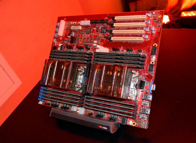
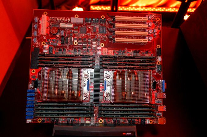
| 11:40p | Early AMD Zen Server CPU and Motherboard Details: Codename ‘Naples’, 32-cores, Dual Socket Platforms, Q2 2017
At the AMD Zen microarchitecture announcement event yesterday, the lid was lifted on some of the details of AMD’s server platform. The 32-core CPU, codename Naples, will feature simultaneous multithreading similar to the desktop platform we wrote about earlier, allowing for 64 threads per processor. Thus, in a dual socket system, up to 128 threads will be available. These development systems are currently in the hands of select AMD partners for qualification and development. AMD was clear that we will expect to hear more over the coming months (SuperComputing 2016 is in November 2016, International SuperComputing is in June 2017) with a current schedule to start providing servers in Q2 2017.
Analysing AMD’s 2P MotherboardAMD showed off a dual socket development motherboard, with two large AMD sockets using eight phase power for each socket as well as eight DDR4 memory slots.
It was not stated if the CPUs supported quad-channel memory at two DIMMs per channel or eight channel memory at this time, and there’s nothing written on the motherboard to indicate which is the case – typically the second DIMM slot in a 2DPC environment is a different color, which would suggest that this is an eight-channel design, however that is not always the case as some motherboard designs use the same color anyway.
However, it is worth noting that each bank of four memory slots on each side of each CPU has four chokes and four heatsinks (probably VRMs) in two sets. Typically we see one per channel (or one per solution), but the fact that each socket seems to have eight VRMs for the memory would also lean into the eight-channel idea. To top it off, each socket has a black EPS 12V (most likely for the CPU), which is isolated and clearly for CPU power, but also a transparent EPS 12V and a transparent 6-pin PCIe connector. These transparent connectors are not as isolated, so are not for low power implementation, but each socket does have one attached, perhaps suggesting that the memory interfaces are powered independently to the CPU. More memory channels would require more power, and four-channel interfaces have been done and dusted before via the single EPS 12V, so requiring even more power raises questions. I have had word in my ear that this may be as a result of support for future high energy memory, such as NVDIMM, although I have not been able to confirm this. Edit: The transparent EPS 12V could be a PCIe 8-pin in retrospect, but still seems excessive for the power it can provide. Unfortunately, we could not remove the heatsinks to see the CPUs or the socket, but chances are this demo system would not have CPUs equipped in the first place. Doing some basic math based on the length of a DDR4 module, our calculations show that the socket area (as delineated by the white line beyond the socket) is 7.46 cm x 11.877 cm, to give an area of 88.59 cm2. By comparison, the heatsink has an active fin floor plan area of 62.6 cm2 based on what we can measure. Unfortuantely this gives us no indication of package area or die area, both of which would be more exciting numbers to have. Putting the CPU, memory and sockets aside, the motherboard has a number of features worth pointing out. There is no obvious chipset or southbridge in play here. Where we would normally expect a chipset, we have a Xilinx Spartan FPGA without a heatsink, although I would doubt this is the chipset based on the fact that there is an ‘FPGA Button’ right above it and this is most likely to aid in some of the debugging elements on the system.
Further to this, the storage options for the motherboard are all located on the left hand side (as seen) right next to one of the CPUs. Eight SATA style ports are here, all in blue which usually indicates that these are part of the same head controller, but also part of the text on the motherboard states ‘ALL SATA CONNS CONNECTED TO P1’ which indicates the first processor (from the main image, left to right, athough P1 is actually the 'second processor') has direct control. Other typical IO on the rear panel such as a 10/100 network port (for the management) and the USB 3.0 ports are next to the second processor, which might indicate that this processor has IO control over these parts of the system. However the onboard management control, provided by an ASpeed AST2500 controller with access to Elpida memory, is nearer the PCIe slots and the Xilinx FPGA. The lack of an obvious chipset, and the location of the SATA ports, would point to Naples having the southbridge integrated on die, and creating an SoC rather than a pure CPU. Bringing this on die, to 14nm FinFET, will allow the functions to be in a lower power process (historically chipsets are created at a larger lithography node to the CPU) as well as adjustments in bandwidth and utility, although at the expense of modularity and die area. If Naples has an integrated chipset, it makes some of the findings on the AM4 platform we saw at the show very interesting. Either that or the FPGA is actually used for the developers to change southbridge operation on the fly (or that chipsets are actually becoming more like FPGAs, which is more realistic as chipsets move to PCIe switch mechanisms). There are a lot of headers and jumpers on board which won’t be of much interest to anyone except the platform testing, but the PCIe layout needs a look. On this board we have four PCIe slots below one of the CPUs, each using a 16 lane PCIe slot. By careful inspection of the pins we can certainly tell that the slots are each x16 electrical.
However the highlighted box gives some insight into the PCIe lane allocation. The text says:
“Slot 3 has X15 PCIe lanes if MGMT PCIe Connected This would indicate that slot three has a full x16 lane connection for data, or in effect we have 64 lanes of PCIe bandwidth in the PCIe slots. That’s about as far as we can determine here – we have seen motherboards in the past that take PCIe lanes from both CPUs, so at best we can say that in this configuration that the Naples CPU has between 32 lanes and 64 lanes for a dual processor system. The board traces, as far as we were able to look at the motherboard, did not make this clear, especially when this is a multi-layer motherboard (qualification samples are typically over-engineered anyway). There is an outside chance that the integrated southbridge/IO is able to supply an x16 combination PCIe lane, however there is no obvious way to determine if this is the case (and is not something we’ve seen historically). AM4 Desktop MotherboardsElsewhere on display for Zen, we also saw some of the internal AM4 motherboards in the base units at the event.
These were not typical motherboard manufacturer boards from the usual names like ASUS or GIGABYTE, and were very clearly internal use products. We weren’t able to open up the cases to see the boards better, but on closer inspection we saw a number of things. First, there were two different models of motherboards on show, both ATX but varying a little in the functionality. One of the boards had twelve SATA ports, some of which were in very odd locations and colors, but we were unable to determine if any controllers were on board. Second, each of the boards had video outputs. This would be because we already know that the AM4 platform has to cater for both Bristol Ridge and Summit Ridge, with the former being APU based with integrated graphics and the updated Excavator v2 core design. On one of the motherboards we saw two HDMI outputs and a DisplayPort output, suggesting a full 3-digital display pipeline for Bristol Ridge.
The motherboards were running 2x8GB of Micron memory, running at DDR4-2400. Also, the CPU coolers – AMD was using both its 125W AMD Wraith cooler as well as the new 95W near silent cooler between all four/five systems on display. This pegs these engineering samples at a top end of this TDP, but if recent APU and FX product announcements are anything to go by, AMD is happy to put a 125W cooler on a 95W CPU, or a 95W cooler on a 65W CPU if required.
I will say one thing that has me confused a little. AMD has been very quiet on the chipset support for AM4, and what IO the south bridge will have on the new platform (and if that changes if a Bristol or Summit Ridge CPU is in play at the time). In the server platform, we concluded above that the chipset is likely integrated into the CPU – if that is true on the consumer platform as well, then I would point to the chipset-looking device on these motherboards and start asking questions. Typically the chipset on a motherboard is cooled by a passive heatsink, but these chips here had low z-height on fans them and were running at quite the rate. I wonder if they were like this so when the engineers use the motherboards it means there is more space to plug testing tools, or if it for another purpose entirely. As expected, AMD said to expect more information closer to launch. Wrap UpTo anyone who says motherboards are boring, well I think AMD has given a number of potential aspects of the platform away in merely showing a pair of these products for server and desktop. Sure, they answer some questions and cause a lot more of my hair to fall out trying to answer the questions that arise, but at this point it means we can start to have a fuller understanding of what is going on beyond the CPU. As for server based Zen, Naples, depending on PCIe counts and memory support, along with the cache hierarchy we discussed in the previous piece, the prospect of it playing an active spot in enterprise seems very real. Unfortunately, it is still a year away from launch. There are lots of questions about how the server parts will be different, and how the 32-cores on the SKUs that were talked about will be arranged in order to shuffle memory around at a reasonable rate – one of the problems with large core count parts is being able to feed the beast. AMD even used that term in their presentation, meaning that it’s clearly a topic they believe they have addressed.
| |||||||||||||||||||||||||||||||||||||||||||||||||||||||||||||||||||||||||||||||||||||||||||||||||||||||||||||||||||||||


| << Previous Day |
2016/08/18 [Calendar] |
Next Day >> |