[Most Recent Entries] [Calendar View]
Thursday, August 25th, 2016
| Time | Event | ||||||||||||||||||||||||||||||||||||||||||||||||||||||||||||||||||||||||||||||||||||||||||||||||||||||||||||||||||||||||||||||||||||||||||||||||||||||||||||||||||||||||||||||||||||||||||||||||||||||||||||||||||||||||||||||||||||||||
| 8:00a | Zotac ZBOX MAGNUS EN980 SFF PC Review - An Innovative VR-Ready Gaming Powerhouse The PC market has been subject to challenges over the last several years. However, gaming systems and small form-factor (SFF) PCs have weathered the storm particularly well. Many vendors have tried to combine the two, but space constraints and power concerns have ended up limiting the gaming performance of such systems. Zotac, in particular, has been very active in this space with their E-series SFF PCs. The Zotac ZBOX MAGNUS EN980 that we are reviewing today is the follow-up to last year's MAGNUS EN970 that combined a Broadwell-U CPU with a GTX 970M (rebadged as a GTX 960). The EN980's full-blown 65W Core i5-6400 Skylake desktop CPU and a no-holds barred VR-ready desktop GTX 980 coupled with an all-in-one watercooling solution seem to have addressed the EN970's shortcomings. Read on to find out how the unit performs in our rigorous benchmarking and evaluation process. | ||||||||||||||||||||||||||||||||||||||||||||||||||||||||||||||||||||||||||||||||||||||||||||||||||||||||||||||||||||||||||||||||||||||||||||||||||||||||||||||||||||||||||||||||||||||||||||||||||||||||||||||||||||||||||||||||||||||||
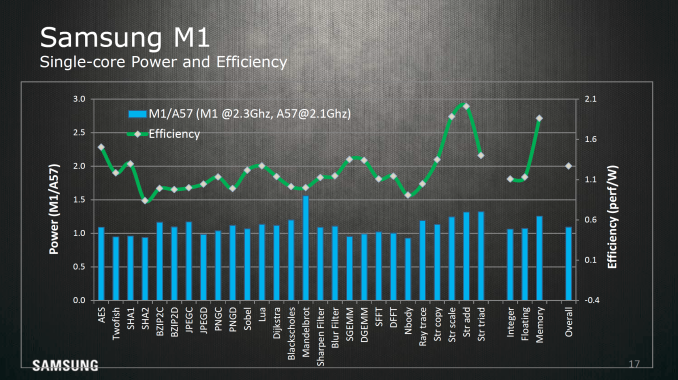
| 8:00a | Hot Chips 2016: Exynos M1 Architecture Disclosed
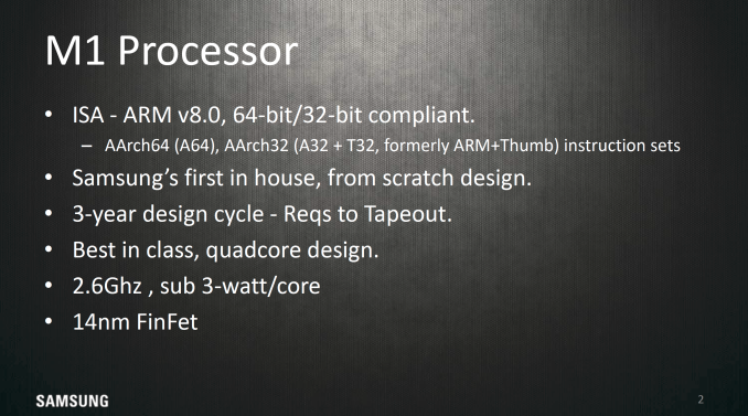
While we can always do black-box testing to try and get a handle for what a CPU core looks like, there’s really only so much you can do given limited time and resources. In order to better understand what an architecture really looks like a vendor disclosure is often going to be as good as it gets for publicly available information. The Exynos M1 CPU architecture is Samsung’s first step into a custom CPU architecture for an mobile SoC. Custom CPU architectures are hardly a trivial undertaking, so it’s unlikely that a company would make the investment solely for a marketing bullet point.
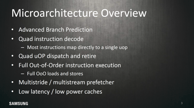
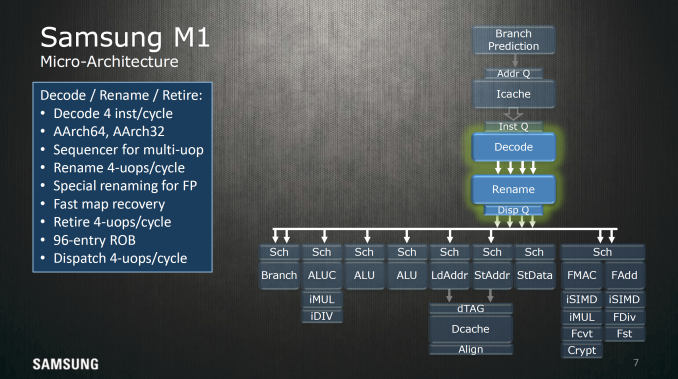
With that said, Samsung has provided some background for the Exynos M1, claiming that the design process started about 3 years ago in 2013 around the time of the launch of the Galaxy S4. Given the issues that we saw with Cortex A15 in the Exynos 5410, it's not entirely unsurprising that this could have been the catalyst for a custom CPU design. However, this is just idle speculation and I don't claim to have any knowledge of what actually led to Exynos M1. At a high level, Samsung pointed out that the Exynos M1 is differentiated from other ARM CPU designs by advanced branch prediction, roughly four instructions decoded per cycle, as well as the ability to dispatch and retire four instructions per cycle. As the big core in the Exynos 8890, it obviously is an out of order design, and there are some additional claims of multistride/stream prefetching and improved cache design.
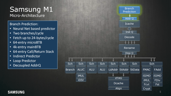
Starting with branch prediction, the major highlight point here is that the branch predictor uses a perceptron of sorts to reduce the rate at which branches miss. If you understand how pipelining works, it takes a significant amount of time to reload saved state and invalidate the execution that occurred after an incorrect branch. I’m no expert here but it looks like this branch predictor also has the ability to do multiple branch predictions at the same time, either as a sort of multi-level branch predictor or handling multiple successive branches. Perceptron branch prediction isn't exactly new in academia or in real-world CPUs, but it's interesting to see that this is specifically called out when most companies are reluctant to disclose such matters.
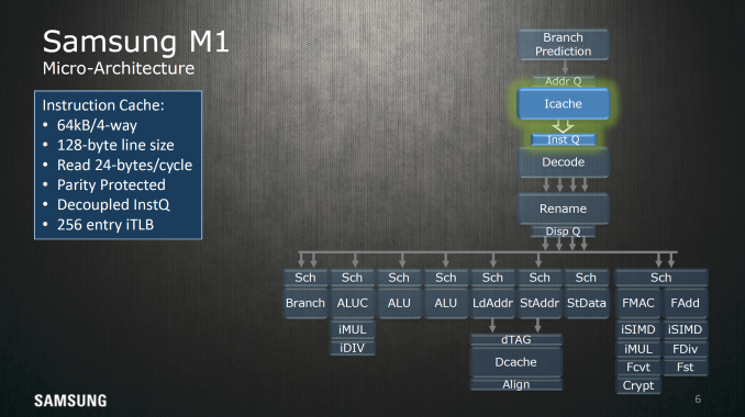
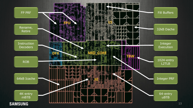
Moving past branch prediction we can see some elements of how the cache is set up for the L1 I$, namely 64 KB split into four sets with 128-byte line sizes for 128 cache lines per set, with a 256 entry TLB dedicated to faster virtual address translation for instructions. The cache can read out 24 bytes per cycle or 6 instructions if the program isn’t using Thumb instruction encoding.
On the instruction side we find decode, rename, and retire stages, register rename logic. The decode stage can handle up to 4 instructions per clock while the retire, and dispatch systems are all capable of handling four instructions every cycle, so best case throughput is going to be four instructions per cycle assuming the best-case scenario that the ARM instruction is a single micro-operation. Other areas of interest include the disclosure of a 96 entry reorder buffer, which defines how many instructions can be in-flight at any given time. Generally speaking more entries is better for extracting ILP here, but it’s important to understand that there are some significant levels of diminishing returns in going deeper, so doubling the reorder buffer doesn’t really mean that you’re going to get double the performance or anything like that. With that said, Cyclone’s reorder buffer size is 192 entries and the Cortex A72 has 128 entries, so the size of this buffer is not really anything special and is likely a bit smaller in order to cut down on power consumption.
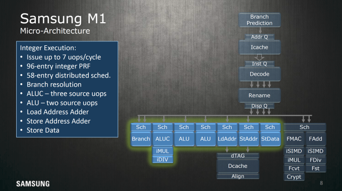
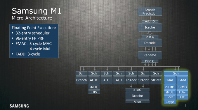
For integer execution the Exynos M1 has seven execution ports, with most execution pipelines getting their own dedicated schedulers. It's to be noted that the branch monitor is able to be fed 2 µops per cycle. On the floating point side it looks like almost everything shares a single 32 entry scheduler, which can do a floating point multiply-accumulate operation every 5 cycles and a floating point multiplication every 4 cycles. Floating point addition is a 3 cycle operation.
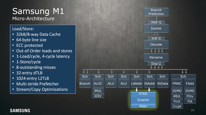
For loads and stores, a 32 KB, 8-way set associative cache with 64 byte line size is used as well as a 32 entry dTLB and 1024 entry L2 dTLB to hold address translations and the associated data for any given address, and allows out of order loads and stores to reduce visible memory latency. Up to 8 outstanding cache misses for loads can be held at any given time, which reduces the likelihood of stalling, and there are additional optimizations for prefetching as well as optimizations for other types of memory traffic.
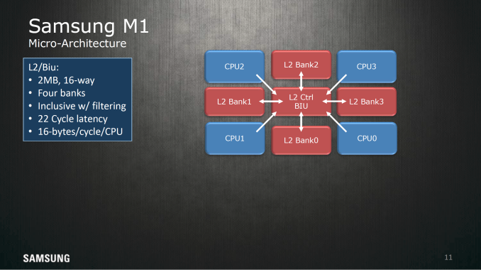
The L2 cache here is 2MB shared across all cores split into 16 sets. This memory is also split into 4 banks and has a 22 cycle latency and has enough throughput to fill two AArch64 registers every cycle, and if you look at the actual floorplan this diagram is fairly indicative of how it actually looks on the die.
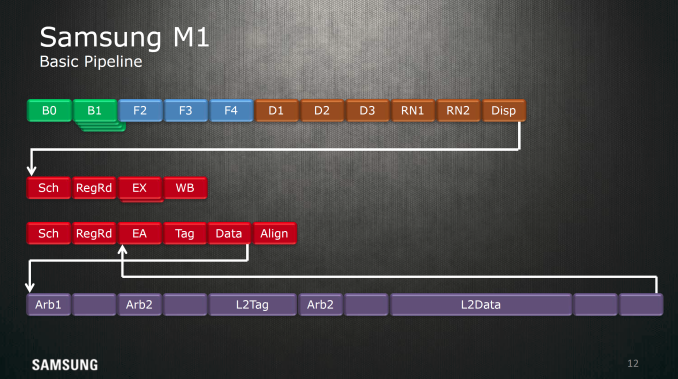
Samsung also highlighted the pipeline of the Exynos M1 CPU at a high level. If you're familiar with how CPUs work you'll be able to see how the basic stages of instruction fetch, decode, execution, memory read/write, and writeback are all present here. Of course, due to the out of order nature of this CPU there are also register rename, dispatch, and scheduling stages.
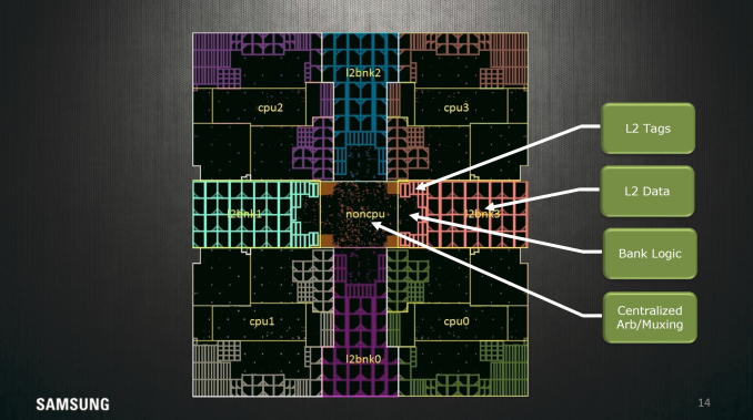
It's fairly rare to see this kind of in-depth floorplanning shots from the designers themselves, so this slide alone is interesting to see. I don't have a ton to comment on here but it's interesting to see the distances of all the components of the CPU from the center of the core where most of the execution is happening.
Overall, for Systems LSI's first mobile CPU architecture it's impressive just how quickly they turned out a solid design in three years from inception to execution. It'll be interesting to see what they do next once this design division really starts to hit its stride. CPU architectures are pipelined to some extent, so even if it takes three years to design one, if the mobile space as a whole is anything to go by then it's likely that we'll be seeing new implementations and designs from this group in the next year or two. Given the improvements we've seen from the Exynos 5420 to 7420 it isn't entirely out of question that we could see much more aggressive execution here in the near future, but without a crystal ball it's hard to say until it happens. | ||||||||||||||||||||||||||||||||||||||||||||||||||||||||||||||||||||||||||||||||||||||||||||||||||||||||||||||||||||||||||||||||||||||||||||||||||||||||||||||||||||||||||||||||||||||||||||||||||||||||||||||||||||||||||||||||||||||||
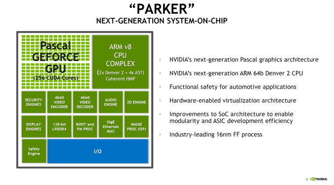
| 11:00a | Hot Chips 2016: NVIDIA Discloses Tegra Parker Details
At CES 2016 we saw that DRIVE PX2 had a new Tegra SoC in it, but to some extent NVIDIA was still being fairly cagey about what was actually in this SoC or what the block diagram for any of these platforms really looked like. Fortunately, at Hot Chips 2016 we finally got to see some details around the architecture of both Tegra Parker and DRIVE PX2.
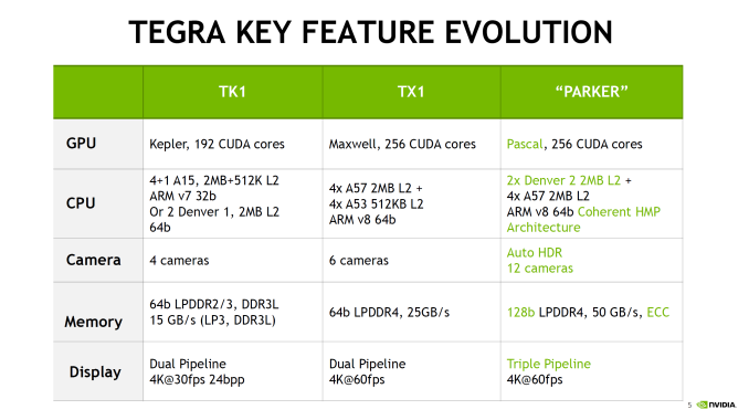
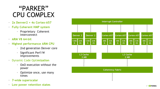
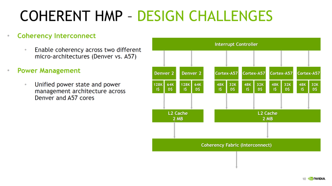
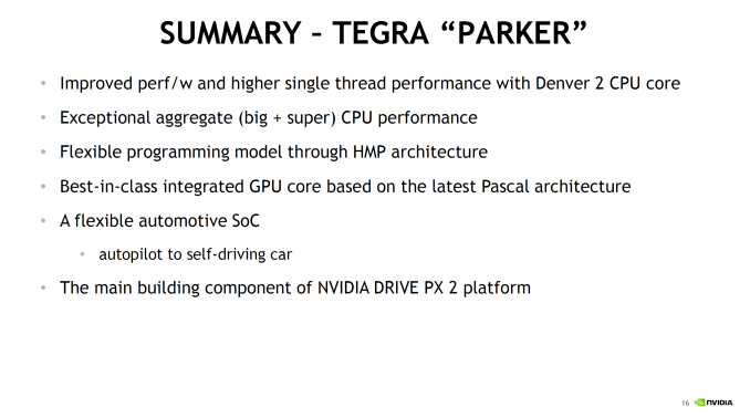
Starting with Parker, this is an SoC that has been a long time coming for NVIDIA. The codename and its basic architectural composition were announced all the way back at GTC in 2013, as the successor to the Logan (Tegra K1) SoC. However Erista (Tegra X1) was later added mid-generation - and wound up being NVIDIA's 20nm generation SoC - so until now the fate of Parker has not been clear. As it turns out, Parker is largely in line with NVIDIA's original 2013 announcement, except instead of a Maxwell GPU we get something based off of the newer Pascal architecture. But first, let's talk about the CPU. The CPU complex has been disclosed as a dual core Denver 2 combined with a quad core Cortex A57, with the entire SoC running on TSMC 16nm FinFET process. This marks the second SoC to use NVIDIA's custom-developed ARM CPU core, the first being the Denver version of the Tegra K1. Relative to K1, Parker (I suspect NVIDIA doesn't want to end up with TP1 here) represents both an upgrade to the Denver CPU core itself, and how NVIDIA structures their overall CPU complex, with the addition of a quartet of ARM Cortex-A57 cores joining the two Denver 2 cores. The big question for most readers, I suspect, is about the Denver 2 CPU cores. NVIDIA hasn't said a whole lot about them - bearing in mind that Hot Chips is not an exhaustive deep-dive style architecture event - so unfortunately there's not a ton of information to work with. What NVIDIA has said is that they've worked to improve the overall power efficiency of the cores (though I'm not sure if this factors in 16nm FinFET or not), including by implementing some new low power states. Meanwhile on the performance side of matters, NVIDIA has confirmed that this is still a 7-wide design, and that Denver 2 uses "an improved dynamic code optimization algorithm." What little that was said about Denver 2 in particular was focused on energy efficiency, so it may very well be that the execution architecture is not substantially different from Denver 1's.
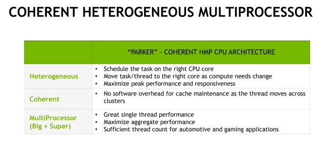
With that in mind, the bigger news from a performance standpoint is that with Parker, the Denver CPU cores are not alone. For Parker the CPU has evolved into a full CPU complex, pairing up the two Denver cores with a quad-core Cortex-A57 implementation. NVIDIA cheekily refers to this as "Big + Super", a subversion of ARM's big.LITTLE design, as this combines "big" A57 cores with the "super" Denver cores. There are no formal low power cores here, so when it comes to low power operation it looks like NVIDIA is relying on Denver. That NVIDIA would pair up Denver with ARM's cores is an interesting move, in part because Denver was originally meant to solve the middling single-threaded performance of ARM's earlier A-series cores. Secondary to this was avoiding big.LITTLE-style computing by making a core that could scale the full range. For Parker this is still the case, but NVIDIA seems to have come to the conclusion that both responsiveness and the total performance of the CPU complex needed addressed. The end result is the quad-core A57 to join the two Denver cores.
NVIDIA didn't just stop at adding A57 cores though; they also made the design a full Heterogeneous Multi-Processing (HMP) design. A fully coherent HMP design at that, utilizing a proprietary coherency fabric specifically to allow the two rather different CPU cores to maintain that coherency. The significance of this - besides the unusual CPU pairing - is that it should allow NVIDIA to efficiently migrate threads between the Denver and A57 cores as power and performance require it. This also allows NVIDIA to use all 6 CPU cores at once to maximize performance. And since Parker is primarily meant for automotive applications - featuring more power and better cooling - unlike mobile environments it's entirely reasonable to expect that the design can sustain operation across all 6 of those CPU cores for extended periods of time. Overall this setup is very close to big.LITTLE, except with the Denver cores seemingly encompassing parts of both "big" and "little" depending on the task. With all of that said however, it should be noted that NVIDIA has not had great luck with multiple CPU clusters; Tegra X1 featured cluster migration, but it never seemed to use its A53 CPU cores at all. So without having had a chance to see Parker's HMP in action, I have some skepticism on how well HMP is working in Parker.
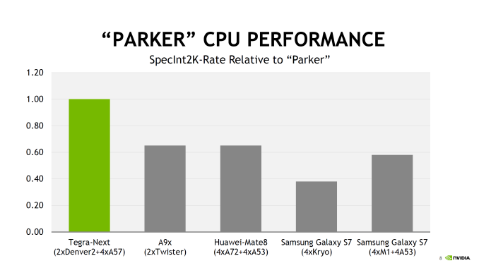
Overall, NVIDIA is claiming about 40-50% more overall CPU performance than A9x or Kirin 950, which is to say that if your workload can take advantage of all 6 CPUs in the system then it’s going to be noticeably faster than two Twister CPUs at 2.2 GHz. But there’s no comparison to Denver 1 (TK1) here, or any discussion of single-thread performance. Though on the latter, admittedly I'm not sure quite how relevant that is for NVIDIA now that Parker is primarily an automotive SoC rather than a general purpose SoC.
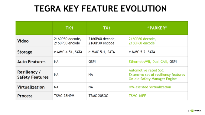
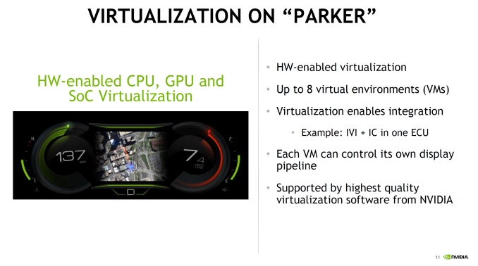
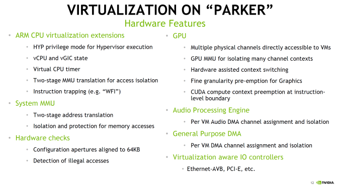
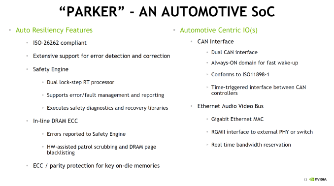
Outside of the CPU, NVIDIA has added some new features to Parker such as doubling memory bandwidth. For the longest time NVIDIA stuck with a 64-bit memory bus on what was essentially a tablet SoC lineup, which despite what you may think from the specs worked well enough for NVIDIA, presumably due to their experience in GPU designs, and as we've since learned, compression & tiling. Parker in turn finally moves to a 128-bit memory bus, doubling the aggregate memory bandwidth to 50GB/sec (which works out to roughly LPDDR4-3200). More interesting however is the addition of ECC support to the memory subsystem. This seems to be in place specfically to address the automotive market by improving the reliability of the memory and SoC. A cell phone and its user can deal with the rare bitflip, however things like self-driving vehicles can't afford the same luxury. Though I should note it's not clear whether ECC support is just some kind of soft ECC for the memory or if it's hardwired ECC (NVIDIA calls it "in-line" DRAM ECC). But it's clear that whatever it is, it extends beyond the DRAM, as NVIDIA notes that there's ECC or parity protection for "key on-die memories", which is something we'd expect to see on a more hardened design like NVIDIA is promoting. Finally, NVIDIA has also significantly improved their I/O functionality, which again is being promoted particularly with the context of automotive applications. There’s more support for extra cameras to improve ADAS and self-driving systems, as well as 4Kp60 video encode, CAN bus support, hardware virtualization, and additional safety features that help to make this SoC truly automotive-focused.
The hardware virtualization of Parker is particularly interesting. It's both a safety feature - isolating various systems from each other - while also allowing for some cost reduction on the part of the OEM as there is less need to use separate hardware to avoid a single point of failure for critical systems. There’s a lot of extra logic going on to make this all work properly, and things like running the dual Parker SoCs in a soft lockstep mode is also possible. In the case of DRIVE PX2 an Aurix TC297 is used to function as a safety system and controls both of the Parker SoCs, with a PCI-E switch to connect the SoCs to the GPUs and to each other. Meanwhile, it's interesting to note that the GPU of Parker was not a big part of NVIDIA's presentation. Part of this is because Parker's GPU architecture, Pascal, has already launched in desktops and is essentially a known quantity now. At the same time, Parker's big use (at least within NVIDIA) is for the DRIVE PX2 system, which is going to be combining Parker with a pair of dGPUs. So in the big picture Parker's greater role is in its CPUs, I/O, and system management rather than its iGPU. Either way, NVIDIA's presentation confirms that Parker integrates a 256 CUDA Core Pascal design. This is the same number of CUDA Cores as on TX1, so there has not been a gross increase in GPU hardware. At the same time moving from TSMC's 20nm planar process to their 16nm FinFET process did not significantly increase transistor density, so there's also not a lot of new space to put GPU hardware. NVIDIA quotes an FP16 rate of 1.5 TFLOPs for Parker, which implies a GPU clockspeed of around 1.5GHz. This is consistent with other Pascal-based GPUs in that NVIDIA seems to have invested most of their 16nm gains into ramping up clockspeeds rather than making for wider GPUs. As the unique Maxwell implementation in TX1 was already closer to Pascal than any NVIDIA dGPU - in particular, it supported double rate FP16 when no other Maxwell did - the change from Maxwell to Pascal isn't as dramatic here. However some of Pascal's other changes, such as fine-grained context switching for CUDA applications, seems to play into Parker's other features such as hardware virtualization. So Pascal should still be a notable improvement over Maxwell for the purposes of Parker.
Overall, it’s interesting to see how Tegra has evolved from being almost purely a mobile-focused SoC to a truly automotive-focused SoC. It’s fairly obvious at this point that Tegra is headed towards higher TDPs than what we’ve seen before, even higher than small tablets. Due to this automotive focus it’ll be interesting to see whether NVIDIA starts to integrate advanced DSPs or anything similar or if they continue to mostly rely on CPU and GPU for most processing tasks. | ||||||||||||||||||||||||||||||||||||||||||||||||||||||||||||||||||||||||||||||||||||||||||||||||||||||||||||||||||||||||||||||||||||||||||||||||||||||||||||||||||||||||||||||||||||||||||||||||||||||||||||||||||||||||||||||||||||||||
| 12:00p | Intel Launches 3D NAND SSDs For Client And Enterprise
Today Intel is announcing a variety of new SSDs with their 3D NAND flash memory. The new models use a mix of 3D MLC and 3D TLC, some SATA and some PCIe, and variously target the consumer, business, embedded and data center markets. While we are still awaiting details on the timing of these product releases, it is clear that Intel is eager to put planar flash behind them. The drive for this is especially strong as the models being replaced are all either based on Intel's relatively expensive 20nm flash or on 16nm flash that Intel had to buy on the open market due to their decision to not participate in the 16nm node at IMFT.
First up, we have a M.2 PCIe SSD branded three different ways for three different markets. In the consumer market we have the SSD 600p series, while the business market will get the Pro 6000p series. The specs released so far differ only in mentioning that the Pro 6000p series will be supported by the remote secure erase feature of Intel's Active Management Technology. The third variant—for the embedded and Internet of Things market—will only get the two smallest capacities, which gives us a look at how this design will perform with the limited parallelism that results from using IMFT's high-capacity 384Gb 3D TLC die.
The 600p and 6000p series are a much more mainstream design than Intel's previous NVMe SSD for the client market. The SSD 750 was a thinly-disguised enterprise drive, with power consumption and physical dimensions that are far too big for the M.2 form factor that has become the preferred choice for client PCIe storage. The SSD 750 was in many ways overkill from the start, and more recent M.2 drives (especially from Samsung) have caught up in peak performance to offer a much better value for typical client usage. The 600p will be going after the client PCIe storage market from the opposite end: as one of the first TLC PCIe SSDs, its performance specifications don't set any records but it will be a much more value-oriented product than any of the M.2 PCIe SSDs currently on the market. Intel has confirmed that the 600p and 6000p are using a third-party controller, and it is most likely Marvell's 88SS1093.
In addition to the SSD E 6000p, there is a new series of SATA drives for the embedded market. The SSD E 5420s series consists of a 240GB 2.5" drive and a 150GB M.2 drive, both with 3D MLC and full power loss protection. The E 5420s is rated for one drive write per day, a substantial improvement over the 0.3 DWPD rating of the E 5410s or the 20GB/day of the E 5400s.
Moving on to the data center products, the SSD DC S3520 is a new mid-range enterprise SATA SSD for read-oriented workloads and the third iteration of the S3500 series. The M.2 form factor has returned as an option after the DC S3510 series was only offered in the 2.5" form factor. As with the SATA drives for the embedded market, performance has decreased but endurance has been bumped up from 0.3 DWPD to 1 DWPD. The larger per-die capacity of the 3D MLC has caused the smallest capacity option to increase from 80GB to 150GB, but 1.6TB is still the largest option for the 2.5" form factor.
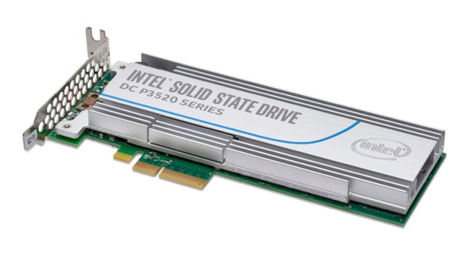
SSD DC S3520 (UPDATED) Finally, for the enterprise PCIe space we have the SSD DC P3520. In March the DC P3320 was announced as Intel's first 3D NAND SSD and the P3520 was mentioned but specifications were not provided at that time. Intel has since decided to only produce the P3520 and to price it close to the level of SATA SSDs. The reduced performance relative to the DC P3500 is a consequence of reduced parallelism at the same capacity that results from using the 256Gb 3D MLC rather than 128Gb 20nm MLC, and the size of this performance regression is a bit dismaying. The DC P3520 is clearly based on the same hardware platform as the rest of the PCIe data center drives, with a familiar layout for the PCB and heatsink evident in the add-in card version.
These new SSDs will have a staggered release over the rest of the year. Starting next week the DC P3520 will be shipping, as well as the 128GB, 256GB and 512GB capacities of the SSD 600p and SSD Pro 6000p. The 2.5" DC S3520 will ship in early September. The rest are planned to be available in Q4. | ||||||||||||||||||||||||||||||||||||||||||||||||||||||||||||||||||||||||||||||||||||||||||||||||||||||||||||||||||||||||||||||||||||||||||||||||||||||||||||||||||||||||||||||||||||||||||||||||||||||||||||||||||||||||||||||||||||||||
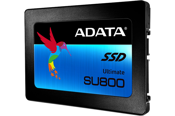
| 6:00p | ADATA Introduces Ultimate SU800 SSD: SMI Controller, 3D NAND, SATA Interface
ADATA has formally introduced its first SSDs based on 3D NAND flash memory. The Ultimate SU800 drives are designed for price-conscious market segments and use SATA interface, which means that they do not offer very high performance. Nonetheless, usage of high-capacity 3D NAND chips helps the manufacturer to increase its MTBF rating and could eventually help ADATA to offer very competitive pricing for these drives. The family of ADATA’s Ultimate SU800 SSDs includes models with 128 GB, 256 GB, 512 GB and 1 TB capacity. The drives are based on Silicon Motion’s SM2258 controller (which has four NAND flash channels and LDPC ECC technology) as well as 3D TLC NAND flash memory from an unknown manufacturer (either IMFT or SK Hynix). The drives come in 2.5”/7 mm form-factor and use SATA 6 Gbps interface. The manufacturer claims that the Ultimate SU800 SSDs support sequential read performance up to 560 MB/s as well as sequential write performance up to 520 MB/s when pseudo-SLC caching is used. The 128 GB model is naturally slower than its brethren are when it comes to writing (up to 300 MB/s), but its read speed is in line with higher-capacity SKUs. ADATA did not mention random performance of the SSDs as well as their power consumption, but the SM2258 controller is capable of up to 90,000 read and up to 80,000 IOPS.
Thanks to higher endurance of 3D TLC NAND compared to planar flash memory made using thin process technologies, ADATA declares 2 million hours MTBF and offers three-year limited warranty on its new SSDs. While the warranty is standard for modern solid-state drives, the MTBF rating 0.5 million hours higher compared to current-generation entry-level SSDs from the company. At present ADATA already has a number of affordable SATA SSDs (e.g., Premier SP550 and SP580) based on planar TLC NAND flash memory. The company specifically noted in its press released that the new Ultimate SU800 will be faster than its existing entry-level models (and will provide higher MTBF). As a result, the new SSDs will be positioned above the currently available inexpensive models. Now, about the retail pricing. ADATA plans to charge $60, $80, $140 and $270 for 128 GB, 256 GB, 512 GB and 1 TB versions of its Ultimate SU800 SSDs, but they are not the cheapest in the company’s model range (even though the price of the 256 GB SKU seems very competitive). Moreover, next month the company plans to introduce another family of 3D NAND-based drives (the Ultimate SU900) with higher performance. | ||||||||||||||||||||||||||||||||||||||||||||||||||||||||||||||||||||||||||||||||||||||||||||||||||||||||||||||||||||||||||||||||||||||||||||||||||||||||||||||||||||||||||||||||||||||||||||||||||||||||||||||||||||||||||||||||||||||||
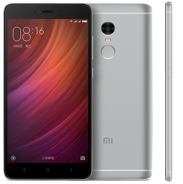
| 6:45p | Xiaomi Launches Redmi Note 4 in China
While we normally don’t cover China-only smartphone releases, Xiaomi is a fairly major player as far as volume as they were one of the first companies in the industry to ship high-end hardware for mid-range prices. We also tend to see that these devices eventually filter out to a more global launch, which The Xiaomi Redmi line has been a solid success pretty much anywhere it shipped, and today Xiaomi launched an update to their Redmi Note line, the Redmi Note 4.
At a high level the Redmi Note 4 is shipping with fairly aggressive specs for the price, which starts at 135 USD for the model with 2GB of RAM and 16GB of internal storage, and 180 USD for the model with 3GB of RAM and 64GB of internal storage.
There’s also a micoSD slot so the 16GB internal storage isn’t necessarily the end of the world.
All SKUs ship with MediaTek’s Helio X20 SoC, but instead of a 2.5 GHz Cortex A72 at the high end it looks like Xiaomi is shipping a 2.1 GHz variant which could either be downclocked deliberately to reduce peak power consumption or a cost saving measure. To try and push for as much battery life as possible, Xiaomi has also shipped a 15.7 WHr battery in this device or 4100 mAh which is probably partially to offset the use of an SoC on a planar 20nm process, and also because most of the people buying phablets are likely doing so due to the battery life benefits. This battery is charged through conventional quick charge at 10W, so charge time may be a bit on the long side but I wouldn’t be surprised if this is a move to improve battery longevity and meet the fairly tight cost target.
The display is a 5.5 inch 1080p unit with a claimed maximum brightness of 450 nits, contrast ratio of 1000:1, and sunlight display technology similar to Apical’s Assertive Display which dramatically improves outdoor visibility beyond what you might expect from a display of that brightness. There’s a mention of 72% NTSC gamut which leads me to believe that this is targeting sRGB fairly well depending upon display settings similar to the Mi Note and Mi Note Pro.
The rear camera is a 13MP unit with PDAF and the front facing camera is a 5MP sensor. Both have an f/2.0 aperture but I don’t really see any mentions of the supplier of the module or sensor here. I suspect that this is going to be a Samsung ISOCELL sensor or something similar on the rear but absent actual data this is just a wild guess.
As far as connectivity goes 802.11a/b/g/n/ac, WiFi Direct, and Bluetooth 4.2 are supported. There’s no explicit discussion of NFC connectivity but seeing as how Mi Pay and AliPay is supported as an NFC-based mobile payments service the Redmi Note 4 should support NFC. For cellular connectivity LTE category 6 and VoLTE are supported, and looking at Xiaomi’s page it looks like GSM bands 2/3/8, WCDMA bands 1/2/5/8, TD-SCDMA bands 34/39, FDD-LTE bands 1/3/5/7/8, and TD-LTE bands 38/39/40/41 are supported for this specific variant. There’s also a mention of support for CDMA2000/1X BC0 which is interesting to see. Dual SIM is supported but when using two SIMs it isn’t possible to use microSD. GPS, GLONASS, and Beidou are supported as GNSS constellations, and there’s an IR port, gyro, accelerometers, proximity sensors, ambient light sensor for auto brightness, and a magnetic hall sensor for things like flip covers. All of this is packaged into a phone that is 151x76x8.35mm and weighs 175 grams, which is actually fairly impressive considering its size, the aluminum unibody, and 15.7 WHr battery. The only real spec out of place at a high level is the lack of USB-C reversible connector, but microUSB is acceptable given the price.
Putting aside the specs, this is actually looking to be a fairly promising phone. We can talk about whether Xiaomi is copying Apple or not, but the Redmi Note 4 seems to have a fairly unique design due to its rear camera placement and the use of a large circular lens somewhat reminiscent of HTC designs, but combines with a dual color LED mounted just below the camera and a fingerprint scanner that appears to be identical in shape to the camera lens between the two. The design of the Redmi Note 4 looks great considering the price, and there’s some irony in that for all of the marketing bluster surrounding the Note7’s symmetrical design, the Redmi Note 4 has visibly better overall ID detailing and overall symmetry. The use of the 2.5D glass, chamfered edges, and slightly curved back should also make for solid ergonomics while allowing for things like tempered glass screen protectors. The fingerprint scanner also is said to be one that allows for learning such that it extends the map of your fingerprints over time to allow for faster, more reliable use. MIUI 8 also has some interesting new features such as the ability to enter either a standard or private user mode depending upon the password/PIN/pattern you enter similar to a KNOX secure folder.
Overall, the Redmi Note 4 from a distance looks to be a fairly impressive phone. It wasn’t all that long ago that things like aluminum unibody design, fast-focusing rear cameras, high quality, high density displays, and fingerprint scanners were impossible to find in a single package for a phone under 200 USD, and Xiaomi has managed to ship a phone with all of these things. It’ll be interesting to see how they manage the transition for the Redmi Note 4 to a global audience, which would likely mean a Qualcomm SoC and new RF front-end, but it’ll be interesting to see all the same. The Xiaomi Redmi Note 4 will be available in China in silver, gold, and gray, and the 2/16GB variant will retail for 899 RMB or 135 USD, and the 3/64GB variant for 1199 RMB or 180 USD. | ||||||||||||||||||||||||||||||||||||||||||||||||||||||||||||||||||||||||||||||||||||||||||||||||||||||||||||||||||||||||||||||||||||||||||||||||||||||||||||||||||||||||||||||||||||||||||||||||||||||||||||||||||||||||||||||||||||||||


| << Previous Day |
2016/08/25 [Calendar] |
Next Day >> |