[Most Recent Entries] [Calendar View]
Tuesday, August 30th, 2016
- Dr Ian Cutress, Host, Senior Editor (@IanCutress)
- Ryan Smith, Editor-in-Chief, (@RyanSmithAT)
| Time | Event | ||||||||||||||||||||||||||||||||
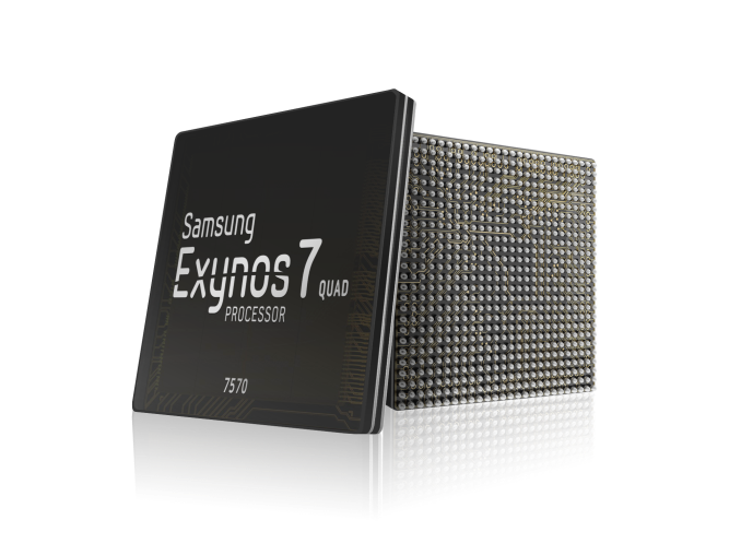
| 6:00a | Samsung Announces Exynos 7570 14nm Budget SoC
Today Samsung LSI launches a new 14nm SoC oriented at the budget and IoT segments. The new Exynos 7570 seems to be a a successor to the Exynos 3470 and Exynos 3475 found in a few of Samsung's budget lineups such as the Galaxy S5 Mini. The chip is a quad-core A53 setup which is said to improve performance by 70% and power efficiency by 30% over its predecessor, although exact clocks weren't publicized. Equally not specified was the GPU, although because of the advertised maximum 1280x800 resolution capabilities of the display pipeline, I wouldn't expect anything more than a very small implementation of a low-end Mali series. The more interesting aspects of this new SoC is its connectivity features as not only does it feature an integrated UE Category 4 modem with 2x carrier aggregation capabilities, but it also as far as I know for the first time for S.LSI integrates WiFi, Bluetooth, FM and GNSS capabilities, features that have traditionally been left in the charge of dedicated solutions such as Broadcom WiFi SoCs (Which following the acquisition by Avago have exited that business segment).
Earlier this year we were surprised to see Samsung announce a 14nm mid-range product as we weren't expecting the economics of the new FinFET manufacturing processes to work out for anything other than flagships SoCs, but soon after Qualcomm followed suit with their own 14nm mid-range SoC. Today's announcement seems to further dispell the doom & gloom over FinFET manufacturing cost as the Exynos 7570's stictly low-end and IoT orientation makes it the first budget SoC on the new process and something as I see as a positive development as the industry continues to shift to full FinFET lineups. | ||||||||||||||||||||||||||||||||
| 7:00a | The AnandTech Podcast, Episode 37: IDF 2016, Alloy, Joule, Broxton, and AMD Zen
Today’s podcast covers the show known as the Intel Developer Forum, or IDF for short. IDF is an annual event focusing on new Intel technologies and product visions, showcasing what is new from small maker-like ‘Internet of Things’ devices all the way up to server platforms and everything in-between. Ian and Ryan were at the show, with plenty of meetings on tap. We found some time to put our thoughts on the announcements in a microphone. The AnandTech Podcast #37: IDF 2016The AnandTech Podcast - Episode 37
| ||||||||||||||||||||||||||||||||
| 9:00a | Intel Announces 7th Gen Kaby Lake: 14nm PLUS, Six Notebook SKUs, Desktop coming in January When Intel first announced the shift from the dual-stage ‘Tick-Tock’ methodology that had driven their core CPU design teams for over a decade into the three-way ‘Process, Architecture, Optimization’ paradigm, there were questions as to how much of the final stage, the Optimization, would actually change the way CPUs were presented or offer upgrades in performance. At the time, ‘Kaby Lake’ as the name for Intel’s third crack at their 14nm process was well known, but users wondered if it was just another Devil’s Canyon (better overclocking) or a full on CPU launch. Well the answer is the latter, and the launch is staggered between today and January. Roll on Kaby Lake. Is that Kah-bee Lake, or Kay-bee Lake? | ||||||||||||||||||||||||||||||||
| << Previous Day |
2016/08/30 [Calendar] |
Next Day >> |