[Most Recent Entries] [Calendar View]
Tuesday, September 27th, 2016
| Time | Event | |||||||||||||||||||||||||||||||||||||||||||||||||||||||||||||||||||
| 7:00a | Xilinx Launches Cost-Optimized Portfolio: New Spartan, Artix and Zynq Solutions
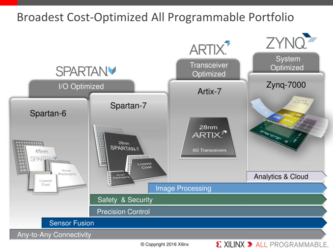
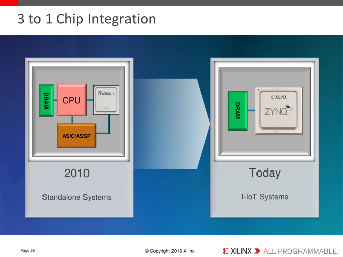
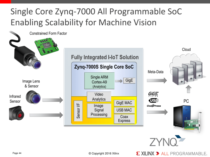
Some of the key elements of the embedded market are cost, power and efficiency. A number of applications for embedded vision and IoT, when applying complexity, rely on the addition of additional fixed function of variable function hardware to accelerate throughput. To that end, the product has multiple FPGA/SoC devices to achieve the goal. The FPGA market is large, however Xilinx is in the process of redefining their product ecosystem to include SoCs with FPGAs built in: silicon with both general purpose ARM processors (Cortex-A series) and programmable logic gates to deal with algorithm acceleration, especially when it comes to sensor fusion/programmable IO and low-cost devices. As a result, Xilinx is releasing a new single-core Zynq 7000 series SoC with an embedded FPGA, as well as new Spartan-7 and Artix-7 FPGAs focused on low cost. The new Spartan-7, built on 28nm TSMC and measuring 8x8mm, is aimed at sensor fusion and connectivity, while the Artix-7 is for the signal processing market. The Zynq-7000 is for the programmable SoC space, featuring a single ARM Core (various models starting with Cortex-A9, moving up to dual/quad Cortex-A53) allowing for on-chip analytical functions as well as host-less driven implementations and bitstream encryption. The all-in-one SoC with onboard FPGA adds a benefit in bringing a floorplan design of multiple chips down from three to one, with the potential to reduce power and offer improved security by keeping the interchip connections on silicon. While the Zynq family isn’t new, the 7000 series for this announcement is aimed squarely at embedded, integrated and industrial IoT platforms by providing a cost-optimized solution.
Gallery: Xilinx Product Specifications
    We spoke with Xilinx’s Steve Glaser, SVP of Corporate Strategy, who explained that Xilinx wants to be in the prime position to tackle four key areas: Cloud, Embedded Vision, Industrial IoT and 5G. The use in the cloud is indicative of high focused workloads that land between ASICs and general purpose compute, but also for networking (Infiniband) and storage, with Xilinx IP in interfaces, SSD controllers, smart networking, video conversion and big data. This coincides with the announcement of the CCIX Consortium for coherent interconnects in accelerators.
Embedded Vision is a big part of the future vision of Xilinx, particularly in automotive and ADAS systems. Part of this involves machine learning, and the ability to apply different implementations on programmable silicon as the algorithms adapt and change over time. Xilinx cites a considerable performance and efficiency benefit over GPU solutions, and a wider range of applicability over fixed function hardware.
Industrial IoT (I-IoT) spans medical, factory, surveillance, robotics, transportation, and other typical industry verticals where monitoring and programmability go hand-in-hand. Steve Glaser cited that Xilinx has an 80% market share in I-IoT penetration, quoting billions of dollars in savings industry wide for very small efficiency gains on the production line.
One thing worth noting that FPGA and mixed SoC/FPGA implementations require substantial software on top to operate effectively. Xilinx plays in all the major computer vision and neural network implementations, and we were told with an aim to streamline compilation with simple pragmas that identify code structures for FPGA implementation. This is where the mixed SoC/FPGA implementations, we are told, work best, allowing the analytics on the ARM cores to adjust the FPGA on the fly as required depending on sensor input or algorithm adjustment. Xilinx sits in that position as being a hardware provider for a solution, but not the end-goal solution provider, if that makes sense. Their customers are the ones that implement what we see in automotive or industrial, so they typically discuss their hardware at a very general level but it still requires an understanding of the markets they focus on to discuss which applications may benefit from FPGA or mixed SoC/FPGA implementations. When visiting any event about IoT or compute as a journalist, there always involves some discussion around FPGA implementation and that transition from hardware to software to product. Xilinx is confident about their position in the FPGA market, and Intel's acquisition of Altera has the markets where both companies used to compete has raised a lot of questions about FPGA roadmaps, with a number of big customers now willing to work on both sides of the fence to keep their options open. On the new cost-optimized chip announcement, the Spartan-7, Artix-7 and Zynq-7000 will be enabled in the 2016.3 release of the Vivado Design Suite and Xilinx SDx environments later this year, with production devices shipping in Q1 2017. Gallery: Xilinx Slide Deck
     
| |||||||||||||||||||||||||||||||||||||||||||||||||||||||||||||||||||
| 9:00a | AMD Announces Embedded Radeon E9260 & E9550 - Polaris for Embedded Markets
While it’s AMD’s consumer products that get the most fanfare with new GPU launches – and rightfully so – AMD and their Radeon brand also have a solid (if quiet) business in the discrete embedded market. Here, system designers utilize discrete video cards for commercial, all-in one products. And while the technology is much the same as on the consumer side, the use cases differ, as do the support requirements. For that reason, AMD offers a separate lineup of products just for this market under the Radeon Embedded moniker. Now that we’ve seen AMD’s new Polaris architecture launch in the consumer world, AMD is taking the next step by refreshing the Radeon Embedded product lineup to use these new parts. To that end, this morning AMD is announcing two new Radeon Embedded video cards: the E9260 and the E9550. Based on the Polaris 11 and Polaris 10 GPUs respectively, these parts are updating the “high performance” and “ultra-high performance” segments of AMD’s embedded offerings.
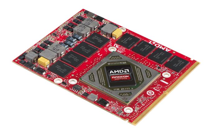
We’ll start things off with the Embedded Radeon E9550, which is the new top-performance card in AMD’s embedded lineup. Based on AMD’s Polaris 10 GPU, this is essentially an embedded version of the consumer Radeon RX 480, offering the same number of SPs at roughly the same clockspeed. This part supersedes the last-generation E8950, which is based on AMD’s Tonga GPU, and is rated to offer around 93% better performance, thanks to the slightly wider GPU and generous clockspeed bump. The E9550 is offered in a single design, an MXM Type-B card that’s rated for 95W. These embedded-class MXM cards are typically based on AMD’s mobile consumer designs, and while I don’t have proper photos for comparison – AMD’s supplied photos are stock photos of older products – I’m sure it’s the same story here. Otherwise, the card is outfitted with 8GB of GDDR5, like the E8950 before it, and is capable of driving up to 6 displays. Finally, AMD will be offering the card for sale for 3 years, which again is par for the course here for AMD. Following up behind the E9550 is the E9260, the next step down in the refreshed Embedded Radeon lineup. This card is based on AMD’s Polaris 11 GPU, and is similar to the consumer Radeon RX 460, meaning it’s not quite a fully enabled GPU. Within AMD’s lineup it replaces the E8870, offering 2.5 TFLOPS of single precision floating point performance to the former’s 1.5 TFLOPS. AMD doesn’t list official clockspeeds for this card, but based on the throughput rating this puts its boost clock at around 1.4GHz. The card is paired with 4GB of GDDR5 on a 128-bit bus.
Meanwhile on the power front, the E9260 is being rated for up to 50W. Notably, this is down from the 75W designation of its predecessor, as the underlying Polaris 11 GPU aims for lower power consumption. And unlike its more powerful sibling, the E9260 is being offered in two form factors: an MXM Type-A card, and a half height half length (HHHL) PCIe card. Both cards have identical performance specifications, differing only in their form factor and display options. Both cards can support up to 5 displays, though the PCIe card only has 4 physical outputs (so you’d technically need an MST hub for the 5th). Finally, both versions of the card will be offered by AMD for 5 years, which at this point would mean through 2021. Moving on, besides the immediate performance benefits of Polaris, AMD is also looking to leverage Polaris’s updated display controller and multimedia capabilities for the embedded market. Of particular note here is support for full H.265 video encoding and decoding, something the previous generation products lacked. And display connectivity is greatly improved too, with both HDMI 2.0 support and DisplayPort 1.3/1.4 support.
The immediate market for these cards will be the same general markets that previous generation products have been pitched at, including digital signage, casino gaming, and medical, all of whom make use of GPUs in various degrees and need parts to be available for a defined period of time. Across all of these markets AMD is especially playing up the 4K and HDR capabilities of the new cards, along of course with overall improved performance. At the same time however, AMD’s embedded group is also looking towards the future, trying to encourage customers to make better use of their GPUs for compute tasks, a market AMD considers to be in its infancy. This includes automated image analysis/diagnosis, machine learning inferencing to allow a casino machine or digital sign to react to a customer, and GPU beamforming for medical. And of course, AMD always has an eye on VR and AR, though for the embedded market in particular that’s going to be more off the beaten path.
Wrapping things up, AMD tells us that the new Embedded Radeon cards will be shipping in the next quarter. The E9260 will be shipping in production in the next couple of weeks, while the E9550 will be coming towards the end of Q4. | |||||||||||||||||||||||||||||||||||||||||||||||||||||||||||||||||||
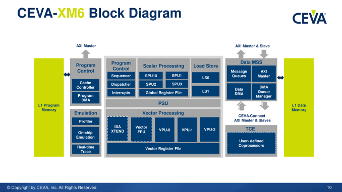
| 9:30a | CEVA Launches Fifth-Generation Machine Learning Image and Vision DSP Solution: CEVA-XM6
Deep learning, neural networks and image/vision processing is already a large field, however many of the applications that rely on it are still in their infancy. Automotive is the prime example that uses all of these areas, and solutions to the automotive 'problem' are require significant understanding and development in both hardware and software - the ability to process data with high accuracy in real-time opens up a number of doors for other machine learning codes, and all that comes afterwards is cost and power. The CEVA-XM4 DSP was aimed at being the first programmable DSP to support deep learning, and the new XM6 IP (along with the software ecosystem) is being launched today under the heading of stronger efficiency, compute, and new patents regarding power saving features. Playing the IP GameWhen CEVA launched the XM4 DSP, with the ability to infer pre-trained algorithms in fixed-point math to a similar (~1%) accuracy as the full algorithms, it won a number of awards from analysts in the field, claiming high performance and power efficiency over competing solutions and the initial progression for a software framework. The IP announcement was back in Q1 2015, with licensees coming on board over the next year and the first production silicon using the IP rolling off the line this year. Since then, CEVA has announced its CDNN2 platform, a one-button compilation tool for trained networks to be converted into suitable code for CEVA's XM IPs. The new XM6 integrates the previous XM4 features, with improved configurations, access to hardware accelerators, new hardware accelerators, and still retains compatibility with the CDNN2 platform such that code suitable for XM4 can be run on XM6 with improved performance. CEVA is in the IP business, like ARM, and works with semiconductor licensees that then sell to OEMs. This typically results in a long time-to-market, especially when industries such as security and automotive are moving at a rapid pace. CEVA is promoting the XM6 as a scalable, programmable DSP that can scale across markets with a single code base, while also using additional features to improve power, cost and performance.
The announcement today covers the new XM6 DSP, CEVA's new set of imaging and vision software libraries, a set of new hardware accelerators and integration into the CDNN2 ecosystem. CDNN2 is a one-button compilation tool, detecting convolution and applying the best methodology for data transfer over the logic blocks and accelerators.
XM6 will support OpenCL and C++ development tools, and the software elements include CEVA's computer vision, neural network and vision processing libraries with third-party tools as well. The hardware implements an AXI interconnect for the processing parts of the standard XM6 core to interact with the accelerators and memory. Along with the XM6 IP, there are hardware accelerators for convolution (CDNN assistance) allowing lower power fixed function hardware to cope with difficult parts of neural network systems such as GoogleNet, De-Warp for adjusting images taken on fish-eye or distorted lenses (once the distortion of an image is known, the math for the transform is fixed-function friendly), as well as other third party hardware accelerators.
The XM6 promotes two new specific hardware features that will aid the majority of image processing and machine learning algorithms. The first is scatter-gather, or the ability to read values from 32 addresses in L1 cache into vector registers in a single cycle. The CDNN2 compilation tool identifies serial code loading and implements vectorization to allow this feature, and scatter-gather improves data loading time when the data required is distributed through the memory structure. As the XM6 is configurable IP, the size/associativity of the L1 data store is adjustable at the silicon design level, and CEVA has stated that this feature will work with any size L1. The vector registers for processing at this level are 8-wide VLIW implementations, meaning 'feed the beast' is even more important than usual.
The second feature is called 'sliding-window' data processing, and this specific technique for vision processing has been patented by CEVA. There are many ways to process an image for either processing or intelligence, and typically an algorithm will use a block or tile of pixels at once to perform what it needs to. For the intelligence part, a number of these blocks will overlap, resulting in areas of the image being reused at different parts of the computation. CEVA's method is to retain that data, resulting in fewer bits being needed in the next step of analysis. If this sounds straightforward (I was doing something similar with 3D differential equation analysis back in 2009), it is, and I was surprised that it had not been implemented in vision/image processing before. Reusing old data (assuming you have somewhere to store it) saves time and saves energy.
CEVA is claiming up to a 3x performance gain in heavy vector workloads for XM6 over XM4, with an average of 2x improvement for like-for-like ported kernels. The XM6 is also more configurable than the XM4 from a code perspective, offering '50% more control'.
With the specific CDNN hardware accelerator (HWA), CEVA cites that convolution layers in ecosystems such as GoogleNet consume the majority of cycles. The CDNN HWA takes this code and implements fixed hardware for it with 512 MACs using 16-bit support for up to an 8x performance gain (and 95% utilization). CEVA mentioned that a 12-bit implementation would save die area and cost for a minimal reduction in accuracy, however there are a number of developers requesting full 16-bit support for future projects, hence the choice.
Two of the big competitors for CEVA in this space, for automotive image/visual processing, is MobilEye and NVIDIA, with the latter promoting the TX1 for both training and inference for neural networks. Based on TX1 on a TSMC 20nm Planar process at 690 MHz, CEVA states that their internal simulations give a single XM6 based platform as 25x the efficiency and 4x the speed based on AlexNet and GoogleNet (with the XM6 also at 20nm, even though it will most likely be implemented at 16nm FinFET or 28nm). This would mean, extrapolating the single batch TX1 data published, that XM6 using AlexNet at FP16 can perform 268 images a second compared to 67, at around 800 mW compared to 5.1W. At 16FF, this power number is likely to be significantly lower (CEVA told us that their internal metrics were initially done at 28nm/16FF, but were redone on 20nm for an apples-to-apples with the TX1). It should be noted that TX1 numbers were provided for multi-batch which offered better efficiency over single batch, however other comparison numbers were not provided. CEVA also implements power gating with a DVFS scheme that allows low power modes when various parts of the DSP or accelerators are idle. Obviously the advantage that NVIDIA has with their solution is availability and CUDA/OpenCL software development, both of which CEVA is attempting to address with one-button software platforms like CDNN2 and improved hardware such as XM6. It will be interesting to see which semiconductor partners and future implementations will combine this image processing with machine learning in the future. CEVA states that smartphones, automotive, security and commercial (drones, automation) applications are prime targets. | |||||||||||||||||||||||||||||||||||||||||||||||||||||||||||||||||||
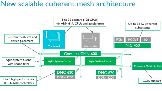
| 11:00a | New ARM IP Launched: CMN-600 Interconnect for 128 Cores and DMC-620, an 8Ch DDR4 IMC
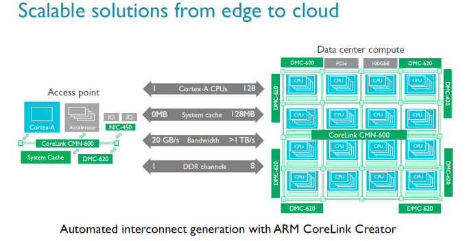
You need much more than a good CPU core to conquer the server world. As more cores are added, the way data moves from one part of the silicon to another gets more important. ARM has announced today a new and faster member to their SoC interconnect IP offerings in the form of CMN-600 (CMN stands for 'coherent mesh network', as opposed to cache coherent network of CCN). This is a direct update to CCN-500 series, which we've discussed at AnandTech before. The idea behind a coherent mesh between cores as it stands in the ARM Server SoC space is that you can put a number of CPU clusters (e.g. four lots of 4xA53) and accelerators (custom or other IP) into one piece of silicon. Each part of the SoC has to work with everything else, and for that ARM offers a variety of interconnect licences for users who want to choose from ARM's IP range. For ARM licensees who pick multiple ARM parts, this makes it easier for to combine high core counts and accelerators in one large SoC.
The previous generation interconnect, the CCN-512, could support 12 clusters of 4 cores and maintain coherency, allowing for large 48-core chips. The new CMN-600 can support up to 128 cores (32 clusters of 4). As part of the announcement, There is also an agile system cache which a way for I/O devices to allocate memory and cache lines directly into the L3, reducing the latency of I/O without having to touch the core.
Also in the announcement is a new memory controller. The old DMC-520, which was limited to four channels of DDR3, is being superseded by the DMC-620 controller which supports eight channels of DDR4. Each DMC-620 channel can contain up to 1 TB DDR4, giving a potential SoC support of 8TB.
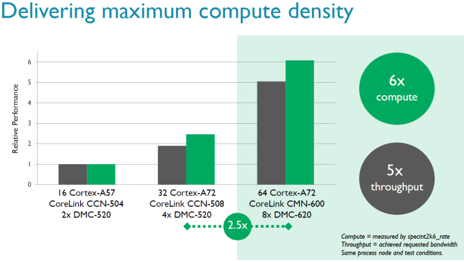
According to ARM through simulations, the improved memory controller offers 50% lower latency and up to 5 times more bandwidth. Also, the new DMC is being advertised as supporting DDR4-3200. 3200 MT/s offers twice as much bandwidth than 1600 MT/s, and doubling the channels offers twice the amount of bandwidth - so we can explain 4 times more bandwidth, so it is interesting that ARM claims 5x more, which would suggest efficiency improvements as well. If you double the number of cores and memory controllers, you expect twice as much performance in the almost perfectly scaling SPEC int2006_rate. ARM claims that their simulations show that 64 A72s will run 2.5 times faster than 32 A72 cores, courtesy of the improved memory controller. If true, that is quite impressive. By comparison, we did not see such a jump in performance in the Xeon world when DDR3 was replaced by DDR4. Even more impressive is the claim that the maximum compute performance of a 64x A72 SoC can go up by a factor six compared to 16x A57 variant. But we must note that the A57 was not exactly a success in the server world: so far only AMD has cooked up a server SoC with it and it was slower and more power hungry than the much older Atom C2000. We have little doubt we will find the new CMN-600 and/or DMC-620 in many server solutions. The big question will be one of application: who will use this interconnect technology in their server SoCs? As most licensees do not disclose this information, it is hard to find out. As far as we know, Cavium uses its own interconnect technology, which would suggest Qualcomm or Avago/Broadcom are the most likely candidates. | |||||||||||||||||||||||||||||||||||||||||||||||||||||||||||||||||||
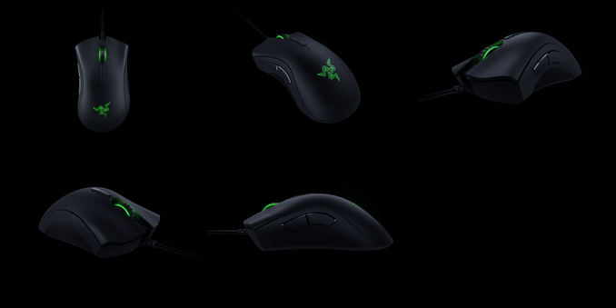
| 11:00a | Razer Updates The DeathAdder Elite Gaming Mouse
Although Razer has become one of the well known gaming computer companies, they got their start with gaming mice, and today Razer is launching their next iteration of the best selling gaming mouse of all time, the Razer DeathAdder Elite. The DeathAdder series was first introduced in 2006. As an iterative update, there could just be some new lights, or what not, but this update brings about a new Razer 5G Optical Sensor, rated for up to 16,000 DPI, which is the highest yet. It can also track at 450 inches per second, which is yet another new standard, and supports up to 50 g of acceleration. Razer is also announcing the DeathAdder Elite has the highest measured resolution accuracy in a gaming mouse at 99.4 percent. If high speed and precision is required, this mouse appears to have that sewn up. The more interesting bit though is that Razer has also upped their game on the switches. Razer has co-designed and produced new mechanical switches with Omron, which are “optimized for the fastest response times” and more importantly to me, an increased durability rating of 50 million clicks. Razer has also included an improved tactile scroll wheel design. I’ve used the DeathAdder in the past, and one of the things that made me abandon it was the scroll wheel, which gave plenty of grip, but would actually wear through the skin on my finger due to the sharp nubs on the wheel. Hopefully the new version is improved in this regard. For fast gaming, the extra grip is likely a nice bonus, but for everyday use I found it uncomfortable.
The overall design hasn’t changed, which is a good thing, since it was a pretty comfortable and ergonomic gaming mouse. It also keeps the Razer Chroma RGB LED lighting system as well, so you can customize away. The mouse has seven programmable buttons, 1000 Hz polling, and a 2.1 m / 7 ft braided USB cable. It weighs in at 105 grams. The mouse is available for pre-order starting today for $69.99 USD, with worldwide shipments starting in October. Source: Razer | |||||||||||||||||||||||||||||||||||||||||||||||||||||||||||||||||||
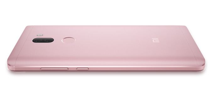
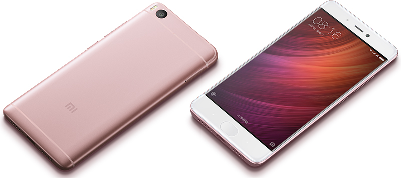
| 5:25p | Xiaomi Mi 5s and Mi 5s Plus Announced
Xiaomi announced two new flagship smartphones today. The Mi 5s and Mi 5s Plus are updates to the Mi 5 / Mi 5 Pro and Mi 5 Plus phones that were announced at MWC 2016 in February, and pack some new hardware inside a new brushed-aluminum chassis. Both the Mi 5s and Mi 5s Plus use Qualcomm’s Snapdragon 821 SoC, which itself is an updated version of the popular Snapdragon 820 that’s inside the Mi 5 phones and many of the other flagship phones we’ve seen this year. With Snapdragon 821, max frequencies increase to 2.34GHz for the two Kryo CPU cores in the performance cluster and 2.19GHz for the two Kryo cores in the power cluster. Complementing the quad-core CPU is Qualcomm’s Adreno 530 GPU that also sees a small 5% increase in peak frequency to 653MHz. While it’s unclear if the 821 includes any changes to its micro-architecture, Qualcomm has likely done some layout optimization as it’s quoting a 5% increase in power efficiency. The Mi 5s and Mi 5s Plus still pair the SoC with LPDDR4 RAM and UFS 2.0 NAND like their predecessors.
The Mi 5s still comes with a 5.15-inch 1080p IPS LCD. This is an extended color gamut panel that will display exceptionally vivid, but inaccurate, colors. Xiaomi claims the display will reach a peak brightness of 600 nits, which it achieves by increasing the number of LEDs in the backlight assembly from the typical 12 to 14 in most edge-lit IPS displays to 16, a feature also shared with the Mi 5. This improves power efficiency by 17%, according to Xiaomi, presumably from using more LEDs at lower individual output levels. The Mi 5s Plus has a larger 5.7-inch 1080p IPS display with a pixel density of 386ppi, which is still decent for an LCD, and a claimed brightness of 550 nits. It's also an extended color gamut panel, but Xiaomi includes an sRGB display mode and the ability to adjust the white point for both the Mi 5s and Mi 5s Plus.
While the front camera still uses a 4MP sensor with large 2.0μm pixels, both new phones receive new rear cameras. The Mi 5s looks to improve low-light performance by using a larger format Sony IMX378 Exmor RS sensor that features 1.55µm pixels; however, image resolution drops to 12MP, the same as Samsung’s Galaxy S7 and Apple’s iPhone 7. The Mi 5s Plus has the more interesting camera setup, employing dual 13MP sensors. Similar to Huawei’s P9 and Honor 8, the Mi 5s Plus uses one sensor for capturing color images and the other sensor for capturing black and white images. The black and white camera lacks an RGB Bayer filter, allowing it to capture more light than a color camera. By combining the output of both sensors, the Mi 5s Plus can theoretically capture brighter images with higher contrast and less noise. The P9 and Honor 8 also use the second camera for measuring depth, aiding camera focusing and allowing the user to adjust bokeh effects after the image is captured, but it’s not clear if the Mi 5s Plus also has these capabilities.
The other big change is a completely new chassis made entirely from brushed aluminum. The back edges are still curved, but there’s no longer any glass or ceramic on the back like the Mi 5 and Mi 5 Pro, respectively. The change to aluminum means the Mi 5s now includes plastic antenna lines on the top and bottom of the back panel. The Mi 5s Plus goes a different route by using plastic inserts at the top and bottom that try to blend in by mimicking the color and texture of the surrounding aluminum.
The Mi 5s Plus includes a circular, capacitive fingerprint sensor on the back that’s slightly recessed, making it easier to locate. The Mi 5s goes the less conventional route with an ultrasonic fingerprint sensor that sits below the edge-to-edge cover glass on the front. Both phones use capacitive buttons rather than onscreen navigation controls and 2.5D cover glass that blends into a chamfered edge on the aluminum frame. Both phones come in four different colors—silver, gray, gold, and pink—and will be available for sale in China starting September 29. | |||||||||||||||||||||||||||||||||||||||||||||||||||||||||||||||||||


| << Previous Day |
2016/09/27 [Calendar] |
Next Day >> |