[Most Recent Entries] [Calendar View]
Tuesday, January 17th, 2017
- Dr Ian Cutress, Host, Senior Editor (@IanCutress)
- Ryan Smith, Editor-in-Chief (@RyanSmithAT)
- Anton Shilov, News Editor (@AntonShilov)
- Matt Humrick, Senior Editor, (@MattHumrick)
- [Qualcomm] Maintains a “no license, no chips” policy under which it will supply its baseband processors only on the condition that cell phone manufacturers agree to Qualcomm’s preferred license terms. The FTC alleges that this tactic forces cell phone manufacturers to pay elevated royalties to Qualcomm on products that use a competitor’s baseband processors. According to the Commission’s complaint, this is an anticompetitive tax on the use of rivals’ processors. “No license, no chips” is a condition that other suppliers of semiconductor devices do not impose. The risk of losing access to Qualcomm baseband processors is too great for a cell phone manufacturer to bear because it would preclude the manufacturer from selling phones for use on important cellular networks.
- Refuses to license standard-essential patents to competitors. Despite its commitment to license standard-essential patents on FRAND terms, Qualcomm has consistently refused to license those patents to competing suppliers of baseband processors.
- Extracted exclusivity from Apple in exchange for reduced patent royalties. Qualcomm precluded Apple from sourcing baseband processors from Qualcomm’s competitors from 2011 to 2016. Qualcomm recognized that any competitor that won Apple’s business would become stronger, and used exclusivity to prevent Apple from working with and improving the effectiveness of Qualcomm’s competitors.
| Time | Event | ||||||||||||||||||||||||||||||||||||||||||||||||||||||||||||||||||||||||||||||||||||||||||||||||||||||||||||||||||
| 7:00a | The AnandTech Podcast, Episode 40: CES 2017 The annual CES show is always a mélange of announcements and sneak peeks for what is to come through the year. At the show we had most of our regular editors on foot, meeting with manufacturers to find out what exactly is going on under the hood. Despite some technical hiccups trying to record the podcast on site, I was able to track down some of our editors for a short burst into their main highlights from CES and thoughts on the year ahead.
The AnandTech Podcast #40: CES 2017FeaturingiTunes Total Time: 1 hour, 48 minutes 26 seconds Outline hh:mm:ss 00:00:00 Start Related ReadingIntel Launches 7th Generation Kaby Lake ASUS Demonstrates ROG Swift PG27UQ: 4K, 144 Hz, HDR, DCI-P3 and G-Sync Dell Announces UP3218K: Its First 8K Display, Due in March Qualcomm Details Snapdragon 835: Kryo 280 CPU, Adreno 540 GPU, X16 LTE | ||||||||||||||||||||||||||||||||||||||||||||||||||||||||||||||||||||||||||||||||||||||||||||||||||||||||||||||||||
| 7:00a | Synaptics at CES 2017: Advanced Touch and DDIC
To some extent, Synaptics is not nearly as visible to consumers as a company like Intel or Qualcomm, but their role in touch interfaces and display driver ICs is a critical part of the user experience. A touchscreen with low processing latency, truly invisible touch sensing, and excellent noise rejection isn’t really what you’ll see on billboards, but if these things aren’t done properly just about anyone will notice the results. Similarly, if a fingerprint scanner has high processing latency and doesn’t have features like learning from a partial match and noise rejection, it’ll be very noticeable if you try a device that has all of these features. Probably the best example of this was the difference in TouchID quality from the iPhone 5s and iPhone 6 to the iPhone 6s and iPhone 7.
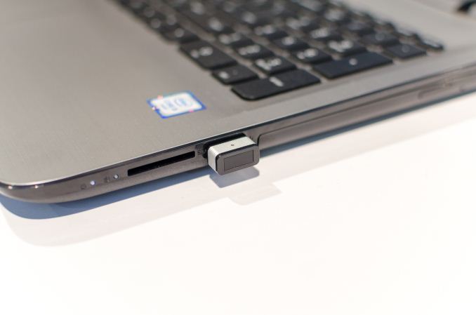
At CES they had a number of new things to show off. The first was a 30 dollar low profile USB fingerprint scanner, which was designed to retrofit laptops and similar devices without a fingerprint scanner in order to enable the use of Windows Hello. I went ahead and tried it and it works flawlessly from what I can see.
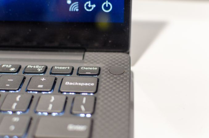
Synaptics is also working on integrating a fingerprint scanner into trackpads and power buttons to enable more seamless designs instead of having a random sensor on the palmrest or somewhere similarly obvious. We also saw their FS4400 and FS4500 fingerprint scanners, which have entered mass production. These sensors enable fingerprint scanning under the glass bezel of a smartphone. There were also prototypes of fingerprint scanners on smart watches, although these prototypes are at an early stage and are more a proof of concept than anything else.
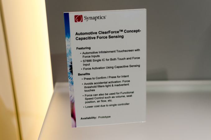
On the automotive side, Synaptics also showed off a neat prototype that enabled force sensing with only four force sensors at the corners of the display. Judging by the state of the prototype this is only for engineering samples at this point, but may have interesting applications.
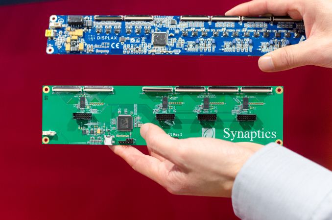
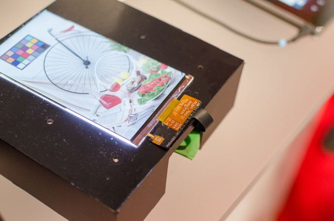
On the DDIC side of things, Synaptics has been working on new solutions for things like large touchscreens. Using technology borrowed from their smartphone designs, they have been able to reduce the number of components and board area needed to enable large touchscreens in applications like mall kiosks.
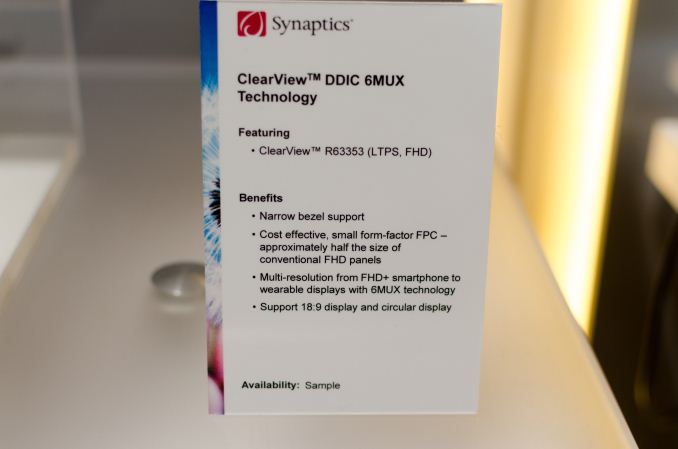
On the mobile side of things, the ClearView R63353 is a DDIC on glass that reduces the amount of bezel that it takes compared to previous display drivers and is currently available for sampling. The Synaptics engineers on site to discuss the issue of bezels did mention that it would be possible to drive down the amount of bezel used by moving to a chip on flex arrangement. However, I suspect that there are other engineering considerations at play as most devices, even those with thin bezels, continue to use a CoG packaging for the DDIC.
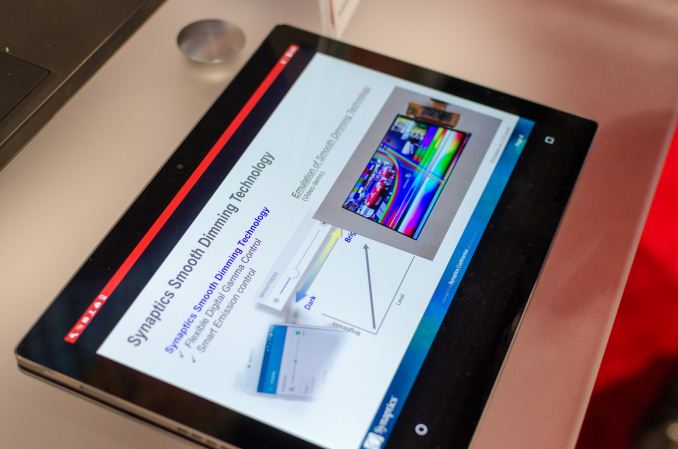
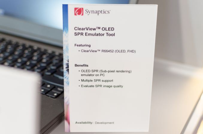
In addition to smaller DDICs, Synaptics has also been working on enabling better OLED displays through new features like smoother dimming and software tools to emulate various subpixel arrangements to determine the best possible subpixel design given design rules. PenTile is mostly here to stay for OLED, but choosing something other than diamond subpixel arrangements can significantly reduce the amount of color shifting when changing viewing angles.
Overall, while Synaptics doesn’t necessarily have the flashiest technologies, the kinds of things that they’re working on remain critical to the end user experience and it’s impressive to see that they continue to iterate and improve upon their products to enable a better user experience. | ||||||||||||||||||||||||||||||||||||||||||||||||||||||||||||||||||||||||||||||||||||||||||||||||||||||||||||||||||
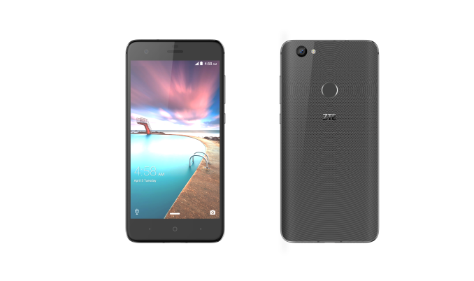
| 9:00a | ZTE's CSX "Hawkeye" Concept Phone Detailed, Kickstarter Launched
For some time now ZTE has been running a program to crowdsource the ideas for smartphones. The basis for this is to collect the ideas of consumers in order to best build the kind of device that consumers want. Some may actually disagree with this philosophy, but it's one that ZTE has taken to its extreme with their crowd sourced X (CSX) program, where X stands for any physically possible mobile device that consumers can dream up. ZTE's CSX program is now beginning to show results with the announcement of ZTE's first crowdsourced smartphone, the Hawkeye. Given that this is a very experimental way of developing a smartphone, ZTE is departing from their standard methods for development and distribution. They've set up a Kickstarter campaign, which for the time being will also serve as the storefront for buyers to purchase the phone. Right now the goal is set at $500,000 USD, and with each phone priced at $200 it appears that ZTE hopes to sell at least 2500 units, which seems feasible even for a very niche device. The two primary features of the Hawkeye phone that came from consumer input are the ability to navigate the interface using eye movement, and the inclusion of an adhesive case that allows the phone to be attached to surfaces. It's worth noting that Samsung has implemented eye-tracking to control the UI in the past, and it hasn't worked out well due to problems with tracking, eye strain, and the general lack of sense in moving a smartphone UI around with ones eyes. The adhesive case is being billed as a convenient feature, and while I don't really see the use of it, it's obviously something that was proposed to ZTE and supported by enough users that it was chosen to be put into production. Until now there hasn't been much detail about the Hawkeye stacks up internally, but we now have an idea of what the specs look like, and I've included those below.
As you can see, there are still some details missing, but the available specs give a good idea as to where the ZTE Hawkeye sits in the market. As of right now there are no true photos of the Hawkeye, partially due to the fact that ZTE is still crowdsourcing ideas regarding the design, including the color choices and the materials to be used, although that latter part will obviously be limited to a degree by the cost of the phone. The cover image for this article is a concept render, and you may have already noted oddities like the fact that it only has a single rear camera when the Hawkeye is supposed to have two. Anyone interested in buying the ZTE Hawkeye can check out ZTE's Kickstarter campaign. It's priced at $199 USD, and ZTE states that they plan to have it available in September of this year, but that date is subject to change. They also caution that they may not be able to deliver the eye-tracking and adhesion features in a satisfactory manner, which could lead to the device being cancelled. In the event of the phone's cancellation, buyers will be entitled to a ZTE phone of equivalent price, with there seemingly being no option to have the contribution refunded instead. | ||||||||||||||||||||||||||||||||||||||||||||||||||||||||||||||||||||||||||||||||||||||||||||||||||||||||||||||||||
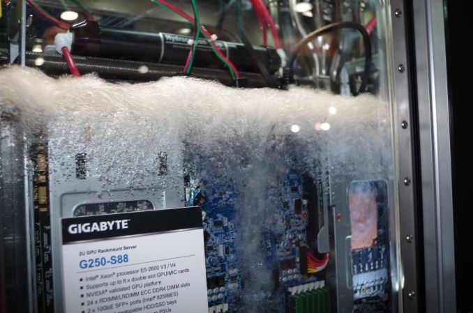
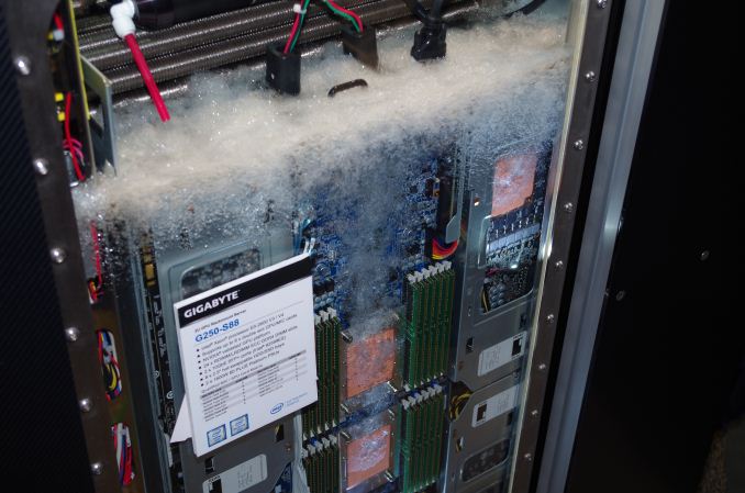
| 10:30a | GIGABYTE Server Shows Two-Phase Immersion Liquid Cooling on a 2U GPU G250-S88 using 3M Novec
In the land of immersed systems, there are many ways of doing things. A few intrepid users have gone with oil, still using a CPU cooler but relying on the liquid cycling throughout the system to remove heat energy. Going back over a decade and a half, I recall a system whereby a 35W processor was immersed, without a heatsink, into a bath of a 3M hydrocarbon with a modest boiling point, around 45C, which was then combined in a sealed system with an external thermal electric cooler to initiate the recycling. The demonstration by GIGABYTE at CES this year with a fully-embedded system is more the latter than the former.
Obviously you cannot use water (unless exceptionally pure/distilled) for conductivity reasons, so some inert hydrocarbon is the purpose here. The concept for this design is a two-phase change from liquid to vapor and back, using no pumps but relying on the fact that the gas will condense and fall back into the solution and sink, causing automatic cycling.
As I mentioned before, previously I had only seen this on a small low powered system, but GIGABYTE and 3M had submerged a full 8-GPU, dual CPU system with 24 memory modules and nothing more than large copper heatsinks on the CPU/GPU, and had even removed the power delivery heatsinks.
To cool the vapor as it rises through the system, a cold radiator is placed inside the sealed system. Well, I say sealed, but during the demo it was being opened and the demonstrator was clearly putting his hand inside. There seemed to also be a system in place to add/remove hydrocarbon material through a pump as well. So the point in all this is more efficient cooling – no need for massive air conditioning units in a data center, no need to pump chilled water into water blocks. I’m surprised that this system was suitable for all that hardware, but it does leave on issue on the table: getting access to replacing hardware. Moving from air to liquid cooling in a data-center always has this issue.
So to keep things under wraps, 3M's Novec line of liquids involve a full array of halogenated hydrocarbon compounds for different uses, and the variant of Novec that is under use here was not specified. However a quick search turns up a likely candidate in Novec 72DA. Novec 72DA liquid is a solution of 70% 1,2-trans-dichloroethylene, 4-16% ethyl nonafluorobutyl ether, 4-6% ethyl nonafluoroisobutyl ether and trace other similar methyl variants. The liquid has a boiling point of 45ºC at very low viscosity (0.4 cP, compared to 0.89 cP for water), but also a low specific heat capacity (1.33 J/g/K, compared to 4.184 for water). Typically water cooling (with blocks) with the high heat capacity is preferred, but at 1.33 J/g/K for the main ingredient in Novec is interesting: take a CPU that uses 140W, and in 60 seconds it will change 8.4 kJ of energy from electricity to heat. That would raise one kg of liquid (0.8 liters, due to 1.257 kg per liter for density) up by 7.24ºC. Thus it would take around 3 minutes from a slightly chilled start to create one kg of the main component of Novec to boiling point. If we add in the latent heat of vaporization, or the energy it takes to transform a chemical from a liquid at boiling point to vapor, then we need another 350 kJ/kg, or 41.67 minutes.
Now obviously in such a system it doesn’t work on pure kilograms of chemical – energy is transferred at larger doses on smaller amounts of liquid at once, causing the effect we see in the photos. | ||||||||||||||||||||||||||||||||||||||||||||||||||||||||||||||||||||||||||||||||||||||||||||||||||||||||||||||||||
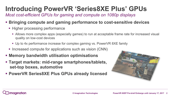
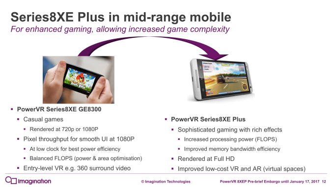
| 11:00a | Imagination Announces PowerVR Series8XE Plus & New Series8XE Designs For Midrange Market
Over the years the PowerVR team over at Imagination has settled in to a rather comfortable release cadence for GPU designs. Every year since the Rogue GPU architecture was initially announced in 2012, the company has released an updated versions of the architecture and/or new GPU designs around the start of the year. Last year’s focus was on high space efficiency with Series8XE, and now for 2017 Imagination is back once again, this time with the aptly named Series 8XE Plus, a new set of GPU core designs specifically for going after the midrange market for 1080p rendering. The launch of the Series8XE Plus family comes as the IP designer has managed to regain better footing in the SoC GPU market. The company has offered the XT and XE lines of GPUs for a few years now, and both have been successful for different reasons. XT of course is the heart of Apple’s A-series SoC GPU designs (albeit not too many other high volume designs), and meanwhile the XE family has become Imagination’s workhorse for the broader market. In terms of the total number of licenses, the high efficiency branch of the Rogue architecture has now become the most successful GPU line for the company since the OpenGL ES 1-era MBX family of the mid-to-late 2000s. As a result, the company is keen to further expand on the family and its success to give their customers what they want.
In terms of design then, Series8XE Plus is intended to fit in the performance gap left between the original Series8XE at the lower-end and Series7XT at the top. The two 8XE SKUs that Imagination introduced last year – the GE8200 and GE8300 – were aimed at the low-end of the market, where fillrate is king. As a result these parts can push a good number of pixels, but only with a limited amount of shading. PowerVR Series8XE Plus then can be best thought of as a rebalancing for the mid-range market, targeting the same fillrates but significantly increasing the number of ALUs paired with that hardware, for more compute throughput in all of its forms.
Architecturally, 8XE Plus is not a significant departure from 8XE, nor would you expect one given the one-year turnaround time and the “Plus” nomenclature. The 8XE Plus USC is identical to the 8XE USC, with the same arrangement of ALUs and pipelines leading to the same basic throughput. Nor have the ROPs (pixel co-processor), the data masters, or the non-core (hardware virtualization and such) features changed. What has been updated is the memory interface and adjacent links: Imagination has tweaked them to match modern LPDDR4 data burst sizes, as LPDDR4 doubles the amount of data fetched per memory clock. This is very similar to what Imagination did with 7XT Plus back in 2016, as LPDDR4 prices have reached a point where the newer memory is appearing in midrange devices.
For the resulting SKUs then, Imagination has assembled 3 new designs: GE8320, GE8325, and GE8340. As telegraphed in their naming scheme, these are meant to serve as more powerful versions of the GE8300 introduced last year. All 3 SKUs are what Imagination calls 4 pixel per clock designs – that is, the ROPs process 4 pixels per clock – but they have much more ALU hardware. Relative to GE8300, the GE832x offers 2x the FLOPS, for 64 FP32 FLOPS per clock. Further above that the GR8340 offers 4x the FLOPS, for 128 FP32 FLOPS per clock.
Clockspeeds aside, per-clock the new 8XE Plus designs are now in the lower-bound of the 7XT’s performance range. Though this means that 8XE Plus steps on 7XT’s foot a little bit, there’s still a rather big distinction between the two. Whereas 7XT is focused on performance first and foremost (including energy efficiency to sustain that), 8XE Plus remains focused on die size and performance per unit thereof. And of course, 8XE Plus still takes a features-light approach to keep die size down. For Imagination, the ultimate goal of these new SKUs is to better serve the midrange market. The company is expecting 1080p displays to increasingly replace 720p displays in this market over the next few years, and while the company already has designs like the GE8300 to serve this market, that sole SKU made for a one-size-fits-all approach. As a result Imagination has rolled out the 8XE Plus SKUs to give vendors a selection of 1080p-appropriate GPUs across a wider range of performance levels to suit their needs.
The focus on FLOPS and shading performance this time around is, in turn, based on where Imagination sees customer needs over the next few years. As with the PC space, display resolutions are slow to increase while the amount of work per pixel is much more quickly increasing, which means shader throughput needs to grow more rapidly to match. Consequently, for 8XE Plus, Imagination has doubled/quadrupled the peak shader throughput to match those needs. Meanwhile, though perhaps not the core market for it, Imagination is also looking to grab a bigger piece of the growing VR and AR markets. Even the GE8300 was workable for the most basic Google Cardboard VR experience (e.g. 360 degree videos), but little else. The newer 8XE Plus designs in turn are meant to offer a lot more shader performance so that the hardware can keep up with rendered graphical effects such as AR overlays.
Moving on, while API support hasn’t changed with this release – Imagination likes to tout OpenVX 1.1 compatibility for 8XE Plus, though this is available to all Rogue products – the company is expecting customers to make much greater use of GPU computing over the next few years. We’ve already seen some of this on the high-end with things such as Apple’s facial recognition and image grouping features in iOS 10, and these kinds of features will trickle down over time. As a result phone manufacturers will need more powerful GPUs in order to do this kind of computer vision processing, and this in turn is closely tied to overall GPU compute performance.
Finally, expect to see the new 8XE Plus designs crop up under the hood of the usual consumer electronics devices. Imagination is trying very hard to wrest a bigger piece of the TV and STB market from ARM – whose Mali-4xx designs have done very well – and the 8XE Plus is a big part of that. Similarly, they are also looking to push further into the ADAS/automotive infotainment markets, where 8XE Plus will offer more compute performance for features such as more complex dashboard designs. Series8XE Rides Again: GE8100 & GE8430While the bulk of Imagination’s focus in today’s announcement is on the new Series8XE Plus, the company is also unveiling a pair of new Series8XE designs today. These are the GE8100 and the GE8430.
These new parts follow the fillrate-first mantra of the 8XE line, while extending it above and below the original 8XE parts introduced last year. The GE8100 is a new low-end part pushing a single pixel per clock – essentially half of a GE8200 – and while not explicitly labeled as such, I suspect this will replace the G6020 as the PowerVR GPU design of choice for wearables and other sub-HD resolution devices. Meanwhile at the high-end is the GE8430, which not to be confused with the GE8340 further scales up the 8XE family with a larger-site 8 pixel per clock design. GE8430 appears to primarily be a play at the 4K market, offering an abundance of ROP throughput (and decent enough compute throughput for the resolution) to drive 4K TVs and set top boxes. Not surprisingly then, Imagination is also including some additional TV/STB functionality that isn’t a core 8XE feature. As with the other 8XE parts, Imagination’s value proposition here is that they believe they offer better fillrate per mm2 (and therefore, overall performance per mm2) than competing designs. And while we can’t verify these claims, certainly area efficiency has by far been the biggest draw for the XE GPU families over the last few years.
Wrapping things up, although Imagination does not announce when to expect SoCs utilizing their designs to hit the consumer market, they have already begun to line up licensing deals for their new GPUs. Given the shorter turnaround time of the XE family, I’m expecting we’ll see these designs start appearing in retail products by the end of this year. Gallery: PowerVR Series8XE Presentation
      | ||||||||||||||||||||||||||||||||||||||||||||||||||||||||||||||||||||||||||||||||||||||||||||||||||||||||||||||||||
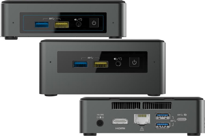
| 2:00p | Intel Officially Launches Baby Canyon NUCs with Kaby Lake: Thunderbolt Makes a Re-entry
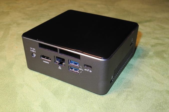
The Baby Canyon NUCs were leaked in July 2016, and Intel officially launched the units at CES 2017. The first-generation NUCs based on Ivy Bridge had a SKU with Thunderbolt support. However, Thunderbolt went missing till it came back in the Skull Canyon NUC (NUC6i7KYK) last year. The Alpine Ridge controller for Thunderbolt 3 also integrates a USB 3.1 Gen 2 controller, making the Type-C Thunderbolt 3 port quite versatile. The Baby Canyon NUCs bring Thunderbolt back into the UCFF NUC form-factor. All the Baby Canyon NUCs have the Alpine Ridge controller. However, the i3 model is limited by firmware, allowing the Type-C port to support only USB 3.1 Gen 2 and Display Port 1.2. The i7 and i5 models have full Thunderbolt 3 support. The leaked specifications we wrote about in July were more or less accurate, and the official specifications allow us to fill in some of the missing blanks. The updated table is presented below. SKUs ending with K are units that do not support a 2.5" drive (only M.2 SSDs are supported).
In terms of appearance, the chassis sides now have a shade of gray to provide a better look when seen along with the black lid. We have a micro-SDXC slot on the side (a full-sized SDXC slot couldn't apparently work with their thermal design). In terms of performance, Kaby Lake should provide the claimed 7 - 11% improvement over the corresponding Skylake products. The new NUCs are also Optane-ready - allowing Optane M.2 SSDs to work seamlessly in conjunction with 2.5" hard drives in the future (when the Optane SSDs come into the market). One important thing to note here is that the i7 model uses a 28W TDP SKU (the Core i7-7567U), compared to the 15W TDP SKUs used in the i3 and i5 models. The i7 and i5 models have Iris Plus graphics with 64MB of eDRAM. None of the Baby Canyon NUCs support vPro. HDMI 2.0 with HDCP 2.2 is supported, thanks to the inclusion of a LSPCon in the BOM. This should make the units into perfect HTPCs with Netflix 4K capability. Compared to the NUCs from the last few generations, these units are not a big upgrade in terms of unique features for other use-cases. Generally speaking, we are not convinced that the Optane-ready feature is a big enough reason to upgrade to the Baby Canyon NUCs. That said, the i7 model should prove pretty interesting to compare against the Broadwell-U Iris NUC.
The NUC7i3BNH with the neutered Alpine Ridge Controller Intel indicated that the kits are slated to come into the market over the next few months at price points similar to the current Skylake versions. While official MSRPs were not provided, we see the NUC7i7BNH for pre-order at $700, the NUC7i5BNH at $610, and the NUC7i3BNH at $496.
| ||||||||||||||||||||||||||||||||||||||||||||||||||||||||||||||||||||||||||||||||||||||||||||||||||||||||||||||||||
| 6:30p | United States FTC Charges Qualcomm with Antitrust Violations over Cellular Modem Patents & Technology
Qualcomm’s legal problems are growing. This afternoon the United States Federal Trade Commission, which has been investigating Qualcomm for possible anti-trust issues since 2014, has moved on to the next stage in their investigating by formally charging the company with multiple antitrust violations. This is the latest in a series of moves from national regulatory authorities, which has seen China, South Korea, and the European Union all fine, settle with, or investigate the company. As with the cases against Qualcomm in other nations, much of FTC’s suit sounds similar: that Qualcomm refused to follow FRAND practices on its patents, and that it used its leverage to force device manufacturers to use its modems by making competing modems more expensive via royalties. Furthermore the FTC also alleges that Qualcomm worked to prevent the adoption of competing (non-LTE) technologies altogether. The FTC summarizes their key points as follows: Points 1 and 2 are fairly straightforward. If Qualcomm was not licensing their patents out at all, or not licensing them under FRAND terms, then that would allow the company to discourage the use of competing modems, either via royalties or the risk of a lawsuit for violating their patents. Qualcomm holds a number of standards-essential patents for both CDMA and LTE, with both network technologies seeing heavy use in the roughly decade-long time period the complaint covers. Similarly, once device vendors agree to use Qualcomm’s chips, Qualcomm is also accused of forcing them to accept the company’s patent licensing terms, which according to the FTC is not a standard industry practice. The end result being that device vendors would be locked into paying higher patent royalties. But perhaps the most interesting – and certainly most novel – aspect of the FTC’s complaint is specifically the company’s agreement with Apple. In their complaint, the FTC alleges that Qualcomm forged a deal with Apple specifically to prevent competitors (e.g. Intel) from getting a foothold in the market and eroding Qualcomm’s dominance. This aspect of the FTC’s complaint also extends to competing technologies, with the FTC further accusing Qualcomm of forging agreements with Apple in part to prevent the adoption of WiMax, which is now a failed standard that was overtaken by the more Qualcomm patent-heavy LTE. Ultimately in filing this complaint, the FTC is looking to force Qualcomm to halt what the commission sees as anticompetitive actions and to ensure a competitive market for cellular modems/basebands. It’s worth noting that as this is just the initial complaint, unless the FTC and Qualcomm were to settle early, this likely will be a multi-year legal battle just to prove or disprove the FTC’s complaints (and that doesn’t include any potential remedies/fines). At the same time, LTE is now well-entrenched and 5G technology is under development, so the market won’t be standing still one way or another while this case is going on. Finally, in response to the FTC’s complaint, Qualcomm has issued their own press release denying the allegations against them. Along with refuting the FCC’s claim that they withheld chips, the company is also voicing their disagreement at the FTC’s underlying legal theory and what they see as a lack of evidence. The company is also questioning the timing of the suit, noting that it comes days before the new presidential administration takes power, insinuating that the suit was filed now to get the case started before the new administration (and its appointed FTC members) took control.
| ||||||||||||||||||||||||||||||||||||||||||||||||||||||||||||||||||||||||||||||||||||||||||||||||||||||||||||||||||


| << Previous Day |
2017/01/17 [Calendar] |
Next Day >> |