[Most Recent Entries] [Calendar View]
Thursday, February 9th, 2017
- Dell Unveils UltraSharp U3417W: Makes Its Curved Display More Curved
- Acer Launches Curved XR382CQK Display: 37.5-inch, 3840×1600, FreeSync, & USB-C
- AOC Announces the AGON AG352UCG 21:9 Curved Display: 35", 3440×1440, 100Hz with G-Sync
- Philips BDM4037UW Goes on Sale: 40 Inch 4K Curved Display for $800
| Time | Event | ||||||||||||||||||||||||||||||||||||||||||||||||||||||||||||||||||||||||||||||||||||
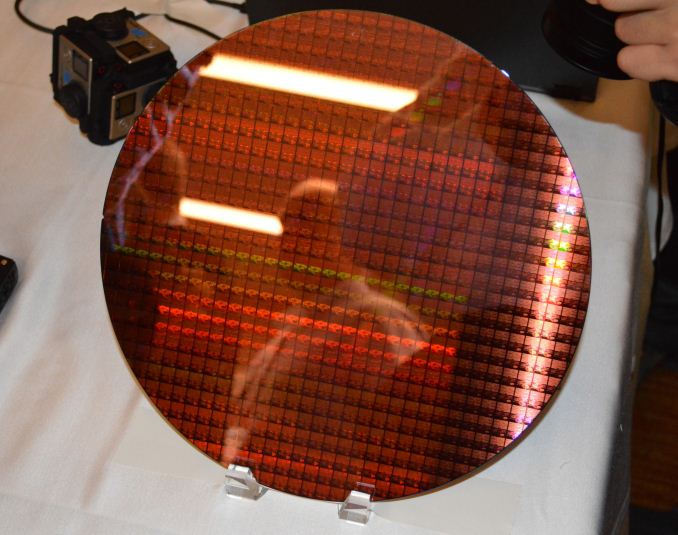
| 4:45p | Intel to Equip Fab 42 for 7 nm
Intel this week announced plans to bring its Fab 42 online to produce semiconductors using a 7 nm fabrication process. It will take three to four years, and the move will cost Intel several billions of dollars but will create approximately 3,000 of high-tech jobs in Chandler, Arizona. Unfortunately, Intel did not share details about its 7 nm manufacturing technology at this time. Intel began construction of its Fab 42 back in 2011 with the aim to build the most advanced, high-volume chip production facility in the world. The building was completed in 2013, but instead of moving in equipment to produce chips using 14 nm fabrication process, Intel decided to postpone its completion in early 2014. The site is equipped with heating, air conditioning, and other essential things, but no actual semiconductor manufacturing equipment has been installed. Intel still has no immediate public plans to use the Fab 42 for the production of chips using its 10 nm process technology in the short-term future but has indicated it intends to use it for its 7 nm ICs several years down the road.
Intel intends to spend as much as $7 billion to equip Fab 42, but at the moment the company does not share what kind of tools it plans to install. As a result we have no new information about Intel's 7 nm technology. Intel has implied that it could start using extreme ultraviolet (EUV) lithography at 7 nm, but has never committed to the plan. Earlier this year the company said it would invest in a 7 nm pilot line in one of its development sites, but did not elaborate beyond that. One of the things that the CEO of Intel disclosed about the 7 nm in general in his email to employees this week is that it requires “an increasing amount of factory space per wafer.” This possibly means that Intel will insert EUV equipment into the process technology for cirical layers and will continue to use a lot of multipatterning, which increases the diversity requirements for the production tools. Intel believes that when completed, Fab 42 will be the most advanced semiconductor wafer fab in the world that will create 3,000 direct high-tech jobs and 10,000 direct and indirect jobs in total. It should be noted that the semiconductor company will not start to move in equipment into the Fab 42 before it figures out all the peculiarities of the 7 nm manufacturing technology. Once it finalizes the pilot line and is satisfied with the equipment performance, it starts to replicate the line at different sites. Intel said that it will use its 7 nm fabrication process to produce various processors for PCs, data centers and other devices that will be used for AI, automated driving, medical research/treatment as well as other applications. So, as usually, the manufacturing technology will be positioned to make the whole stack of Intel’s products several years from now.
Related Reading: | ||||||||||||||||||||||||||||||||||||||||||||||||||||||||||||||||||||||||||||||||||||
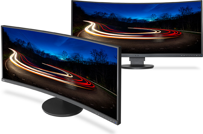
| 6:00p | NEC Goes for a Curved Display, Launches 3440×1440 MultiSync EX341R Monitors
This week NEC has announced its first curved ultrawide display, the EX341R. NEC is promoting the panel for offices, control rooms, trading rooms, and other applications that typically use multi-monitor configurations but also appreciate color accuracy. The screen has a number of differences when compared to displays for gamers, and the price of the new MultiSync EX341R will be reflected in this. In the recent years, NEC concentrated on displays for commercial and professional use, whereas its consumer monitor lineup slowly stepped into the background. The majority of curved ultrawide displays nowadays are designed with gamers in mind, which is why manufacturers tend to incorporate very high refresh rates along with dynamic refresh rate technologies and gaming specific features or aesthetics. Nonetheless, ultrawide displays may make sense to replace those used to multi-monitor environments, and this is a reason why Dell introduced its business-oriented curved ultrawide screens last year. NEC now also sees demand for monitors with a 21:9 aspect ratio from its customers, which is why the company announced its new MultiSync EX341R-BK and EX341R-SV-BK products this week.
The NEC MultiSync EX341R-series displays are based on SVA panels (presumably made by Samsung) with a 3440×1440 resolution, a 1000:1 contrast ratio, 290 nits brightness, 178°/178° viewing angles, 5 ms response time and a 60 Hz refresh rate. It also targets customers that need various degrees of color accuracy (NEC markets the panels as supporting 99.5% sRGB) and therefore bundles the Spyder5 color calibration sensor and the SpectraView II software with the EX341R-SV-BK monitor. As for connectivity, the NEC MultiSync EX341R has one DisplayPort 1.2 with MST support as well as two HDMI headers (one 1.4 and one 2.0). The monitor fully supports NEC’s control Sync technology that allows controlling the settings of up to 25 displays in a multi-monitor setup using controls of only one of them. Additionally, the display supports PBP and PiP features when connected to two computers. Finally, it has a quad-port USB 3.0 hub with two USB Type-B upstream ports (to connect to two different PCs).
The NEC MultiSync EX341R-BK and EX341R-SV-BK displays will be available in February at an MSRP of $999 and $1,149 respectively. Related Reading: | ||||||||||||||||||||||||||||||||||||||||||||||||||||||||||||||||||||||||||||||||||||
| 6:52p | Intel Confirms 8th Gen Core on 14nm, Data Center First to New Nodes
A quick news piece on information coming out of Intel’s annual Investor Day in California. As confirmed to Ashraf Eassa by Intel at the event, Intel’s 8th Generation Core microarchitecture will remain on the 14nm node. This is an interesting development with the recent launch of Intel’s 7th Generation Core products being touted as the ‘optimization’ behind the new ‘Process-Architecture-Optimization’
Despite this, if you were to believe supposed ‘leaked’ roadmaps (which we haven’t confirmed from a second source as of yet), the 8th Generation product ‘Cannon Lake’ is more geared towards the Y and U part of Intel’s roadmap. This would ring true with a mobile first strategy that Intel has mirrored with recent generations such that the smaller, low power chips are off the production line for a new product first, however we'd also expect 10nm to also be in the smaller chips first too (as demonstrated at CES). Where Cannon Lake will end up in the desktop or enterprise segment however remains to be seen. To put something a bit more solid into this, Ashraf also mentioned words from Dr. Venkata ‘Murthy’ Renduchintala, VP and GM of Client and IoT:
If one read too much into this, we may start seeing a blend of process nodes for different segments at the same time for different areas of the market. We already do have that to some extent with the mainstream CPUs and the HEDT/Xeon families, but this phrasing seems that we might get another split between consumer products or consumer and enterprise. We may get to a point where Intel's 'Gen' naming scheme for its CPUs covers two or more process node variants. Speaking of the Enterprise segment, another bit of information has also surfaced, coming from a slide during a talk by Diane Bryant (EVP/GM of Data Center) and posted online by Ashraf. The slide contains the words ‘Data center first for next process node’
We can either talk about process node in terms of the ‘number’, either 14nm/10nm/7nm, or by variants within that process (high power, high efficiency). One might suspect that this means Intel is moving hard and fast with 10nm for Xeons and big computing projects, despite showing off 10nm silicon at CES earlier this year. That being said, it’s important to remember that the data center market is large, and includes high-density systems with many cores, such as Atom cores, and Intel did recently open up its 10nm foundry business to ARM Artisan IP projects. So while the slide does say ‘Data center first’, it might be referring to DC projects based on ARM IP in that segment rather than big 4-24+ core Xeons. At this stage of the game it is hard to tell. On top of all this, Intel still has extreme confidence in its foundry business. An image posted by Dick James of Siliconics from the livestream shows Intel expects to have a three-year process node advantage when its competitors (Samsung, TSMC) start launching 10nm:
I’ve been brief with this news for a reason - at this point there are a lot of balls in the air with many different ways to take this information, and the Investor Day is winding down on talks and finishing with smaller 1-on-1 meetings. We may get further clarification on this news as the day goes on. Update 1: On speaking with Diane Bryant, the 'data center gets new nodes first' is going to be achieved by using multiple small dies on a single package. But rather than use a multi-chip package as in previous multi-core products, Intel will be using EMIB as demonstrated at ISSCC: an MCP/2.5D interposer-like design with an Embedded Multi-Die Interconnect Bridge (EMIB).
Initially EMIB was thought of as a technology relating to Intel's acquisition of Altera and potential future embedded FPGA designs, and given the slide above and comments made at the Investor Day, it seems there are other plans for this technology too. The benefit of using multiple smaller dies over a large monolithic 600mm2 die is typically related to cost and yield, however the EMIB technology also has to be up to par and there may be a latency or compatibility trade-off.
| ||||||||||||||||||||||||||||||||||||||||||||||||||||||||||||||||||||||||||||||||||||
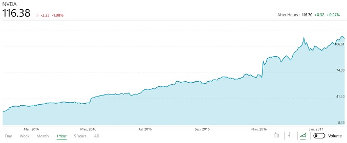
| 10:20p | NVIDIA Reports Q4 2017 And Fiscal 2017 Results: Record Revenue
NVIDIA’s fiscal year for 2017 ended on January 29, 2017, and for the fourth quarter and full year, NVIDIA reports they had record revenues. For Q4 2017, NVIDIA is reporting revenue of $2.173 billio.n, up 55% from a year ago. Gross margin came in at 60.0%, which is up 3.5% from Q4 2016. Operating income for the quarter was $733 million, up 191%, and net income was up 216% to $655 million. The very high growth in operating income and net income are even more impressive, since Q4 2016 was also a record for them at the time. NVIDIA reported $0.99 per share earnings for this quarter, up 183%.
Even though 2016 was a record year for NVIDIA, 2017 was even better. NVIDIA reported record revenue of $6.91 billion for the full fiscal year 2017, which is up 38% from a year ago, and had a net income of $1.666 billion. Earnings per share for the year were $2.57. They also repurchased $739 million in shares over the last year, and paid $261 million in dividends. The majority of NVIDIA’s revenue came from their Gaming segment, which includes their GeForce GPUs. The launch of Pascal has clearly been very successful, and for the quarter NVIDIA’s Gaming segment had revenues of $1.348 billion, up from $810 million a year ago. This is a gain of 66.4% year-over-year, on a market they were already at the top of. This quarter, they also launched the GeForce GTX 1050 and 1050 Ti mobile GPUs, and a new SHIELD TV, along with unveiling the GeForce NOW game streaming service. Professional Visualization had much more modest growth, being up “only” 10.8% from last year, with revenues of $225 million for the quarter. They just launched the GP100 Quadro though, so it may have even more growth to come. Datacenter has been a big focus from NVIDIA in diversifying their portfolio, and this quarter they had some announcements here as well, with a collaboration with Microsoft on the Microsoft Cognitive Toolkit, powered by Microsoft Azure cloud running on NVIDIA DGX-1 deep learning system. They unveiled the DGX SATURNV AI supercomputer, and partnered with the National Cancer Institute and US Department of Energy to build CANDLE to “advance cancer research”. The growth of NVIDIA’s Datacenter segment has been almost exponential, and it is now the second largest source of revenue for the company. For Q4 2017, NVIDIA reported $296 million in revenue from this segment, up from $97 million a year ago, or an increase of 205.1%. NVIDIA has also diversified into Automotive with their Tegra lineup, after originally releasing it as a mobile SoC. This has also been a boon for the company, and they are now powering self-driving cars, and the infotainment systems of major manufacturers like Audi, and Mercedes-Benz, and they’ve partnered with Bosch on self-driving systems as well. This segment saw revenues of $128 million for the quarter, up from $93 million a year ago, or 37.6%. Finally, the OEM and IP segment had revenues of $176 million, down from $198 million a year ago. Unfortunately NVIDIA has not gone into much detail about just why this is dropping, and how revenue from this category breaks down.
For next quarter, NVIDIA is expecting revenues of $1.9 billion, plus or minus 2%, and gross margins between 59.5 and 59.7%. The diversification of NVIDIA from a purely GPU company has clearly paid dividends, especially when their core market is doing as well as it is. The datacenter growth is clearly very high margin as well, considering the jump in net income for the quarter. Source: NVIDIA Investor Relations
| ||||||||||||||||||||||||||||||||||||||||||||||||||||||||||||||||||||||||||||||||||||


| << Previous Day |
2017/02/09 [Calendar] |
Next Day >> |