[Most Recent Entries] [Calendar View]
Friday, June 23rd, 2017
| Time | Event | ||||||||||||||||||||||||||||||||||||||||||||||||||||||||||||||||||||||||||||||||||||||||||||||||||||||||||||||||||||||||||||||||||||||||||||||||||||||||||||||||||||
| 8:00a | FreeTail EVOKE Series CompactFlash Cards Capsule Review
Digital cameras and camcorders employ memory cards (flash-based removable media) for storage of captured content. There are different varieties of memory cards catering to various performance levels. CompactFlash (CF) became popular in the late 90s, but, has now been overtaken by Secure Digital (SD) cards. Despite that, cameras with CF card slots are still getting introduced into the market. Today, we will be taking a look at a couple of CF cards in the EVOKE series from FreeTail Tech. IntroductionCompactFlash (CF) was introduced back in 1994 as a mass storage device format, and it turned out to be the most successful amongst the first set of such products. Electrically, it is based on a parallel ATA (PATA) interface, which means that there is hard transfer rate cap at 167 MBps. However, this is more than sufficient even for current-day 4K video encodes. Having been overtaken by Secure Digital (SD) cards in terms of volume shipment, the price per GB of CF cards is not very attractive. However, certain cameras leave the consumer with no choice. FreeTail Tech is aiming to serve this market segment with the EVOKE series of CF cards - the main push is in terms of value for money. There are two members in the EVOKE series - the EVOKE and EVOKE Pro. The former is the 800x variant, while the Pro is the 1066x variant. There are three capacity points in each - 64GB, 128GB, and 256GB. FreeTail sent over the 800x and 1006x 256GB models for review. Testbed Setup and Testing MethodologyEvaluation of memory cards is done on Windows with the testbed outlined in the table below. The USB 3.1 Type-C port enabled by the Intel Alpine Ridge controller is used for benchmarking purposes on the testbed side. CF cards utilize the Lexar Professional Workflow CFR1 CompactFlash UDMA 7 USB 3.0 Reader. The reader was placed in the Lexar Professional Workflow HR2 hub and uplinked through its USB 3.0 port with the help of a USB 3.0 Type-A female to Type-C male cable.
The full details of the reasoning behind choosing the above build components can be found here. Sequential AccessesFreeTail claims speeds of up to 160 MBps reads and 85 MBps writes for the 800x card. The 1066x one comes in at 160 MBps reads and 150 MBps writes. However, real-world speeds are bound to be lower. For most applications, that really doesn't matter as long as the card is capable of sustaining the maximum possible rate at which the camera it is used in dumps data. We use fio workloads to emulate typical camera recording conditions. We run the workload on a fresh card, and also after simulating extended usage. Instantaneous bandwidth numbers are graphed. This gives an idea of performance consistency (whether there is appreciable degradation in performance as the amount of pre-existing data increases and / or the card is subject to wear and tear in terms of amount and type of NAND writes). Further justification and details of the testing parameters are available here. <select ... ><option ... >Freetail 1066x 256GB</option><option ... >Freetail 800x 256GB</option><option ... >Lexar 1066x 128GB</option> </select>
<select ... ><option ... >Freetail 1066x 256GB</option><option ... >Freetail 800x 256GB</option><option ... >Lexar 1066x 128GB</option> </select>
In the fresh state, the card exhibits very good consistency. The 1066x variant shows that it can handle sustained writes at around 110 MBps, and reads around 135 MBps. The corresponding numbers for the 800x variant are 70 MBps and 130 MBps. The other card that we have evaluated before (the Lexar 1066x 128GB) shows better consistency with reads, though overall benchmark numbers are roughly the same between the two 1066x cards. In the used card scenario, we see that the 800x card has no trouble retaining write consistency, but the 1066x card would occasionally go down to around 80 MBps from the 110 MBps fresh performance number. The read is more interesting. Both cards start off with numbers similar to the fresh case (around 130 MBps), but, end up at around 100 MBps after reading around one-sixth of the card capacity. The Lexar 1066x card doesn't have any such issues AnandTech DAS Suite - Performance ConsistencyThe AnandTech DAS Suite involves transferring large amounts of photos and videos to and from the storage device using robocopy. This is followed by selected workloads from PCMark 8's storage benchmark in order to evaluate scenarios such as importing media files directly into multimedia editing programs such as Adobe Photoshop. Details of these tests from the perspective of memory cards are available here. In this subsection, we deal with performance consistency while processing the robocopy segment. The graph below shows the read and write transfer rates to the memory card while the robocopy processes took place in the background. The data for writing to the card resides in a RAM drive in the testbed. The first three sets of writes and reads correspond to the photos suite. A small gap (for the transfer of the videos suite from the primary drive to the RAM drive) is followed by three sets for the next data set. Another small RAM-drive transfer gap is followed by three sets for the Blu-ray folder. The corresponding graphs for similar cards that we have evaluated before is available via the drop-down selection. <select ... ><option ... >Freetail 1066x 256GB</option><option ... >Freetail 800x 256GB</option><option ... >Lexar 1066x 128GB</option> </select>
Both cards show that they can sustain 25 MBps+ even with a large number of small files. Large files (typical videos) make the card exhibit their best performance. AnandTech DAS Suite - BandwidthThe average transfer rates for each workload from the previous section is graphed below. Readers can get a quantitative number to compare the Freetail 1066x 256GB CF card against the ones that we have evaluated before.
The Lexar 1066x card has a slight edge in the write workloads, but reads often favor the FreeTail cards. We also look at the PCMark 8 storage bench numbers in the graphs below. Note that the bandwidth number reported in the results don't involve idle time compression. Results might appear low, but that is part of the workload characteristic. Note that the same testbed is being used for all memory cards. Therefore, comparing the numbers for each trace should be possible across different cards.
Performance RestorationThe traditional memory card use-case is to delete the files on it after the import process is completed. Some prefer to format the card either using the PC, or, through the options available in the camera menu. The first option is not a great one, given that flash-based storage devices run into bandwidth issues if garbage collection (processes such as TRIM) is not run regularly. Different memory cards have different ways to bring them to a fresh state.Based on our experience, CF cards have to be formatted after all the partitions are removed using the 'clean' command in diskpart. In order to test out the effectiveness of the performance restoration process, we run the default sequential workloads in CrystalDiskMark before and after the formatting. Note that this is at the end of all our benchmark runs, and the card is in a used state at the beginning of the process. The corresponding screenshots for similar cards that we have evaluated before is available via the drop-down selection. <select ... ><option ... >Freetail 1066x 256GB</option><option ... >Freetail 800x 256GB</option><option ... >Lexar 1066x 128GB</option> </select>
We find that CF cards don't have significant performance loss after being subject to our stress test. Therefore, the performance gain from the refresh process is also minimal across all our tested cards. Concluding RemarksThe FreeTail 800x and 1066x cards perform as well as the Lexar 1066x cards for almost all relevant content capture workloads. The Lexar card does have the edge in some of the atypical benchmarks that are part of the PCMark 8 storage bench, but, it is highly unlikely that CF cards are going to be subject to such scenarios (SD cards are a different story, as they are often used in embedded systems and mobile devices). In addition to raw performance and consistency, pricing is also an important aspect. This is particularly important in the casual user and semi-professional markets, where the value for money metric often trumps benchmark numbers. The table below presents the relevant data for the Freetail 1066x and 800x 256GB CF cards and other similar ones that we have evaluated before. The cards are ordered by the $/GB metric.
We find that the FreeTaiil cards handily beat the Lexar one in the value proposition metric. Based on our testing, we have no qualms in recommending either FreeTail card for purchase. Semi-professional and casual users will find the pricing to be very attractive. FreeTail Tech is offering a 10% discount code on Amazon for AnandTech readers. Please enter the code ANAND101 at checkout | ||||||||||||||||||||||||||||||||||||||||||||||||||||||||||||||||||||||||||||||||||||||||||||||||||||||||||||||||||||||||||||||||||||||||||||||||||||||||||||||||||||
| 11:00a | TYAN Shows Two Skylake-SP-Based HPC Servers with Up to 8 Xeon Phi/Tesla Modules
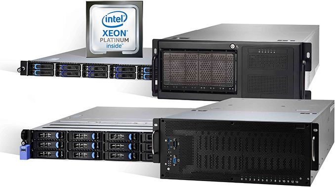
At ISC 17 this sweek, TYAN has demonstrated two new HPC servers based on the latest Intel Xeon processors for high-performance computing and deep learning workloads. The new HPC machines can integrate four or eight Intel Xeon Phi co-processors or the same number of NVIDIA Tesla compute cards, as well as over 10 storage devices. The new TYAN FT77D-B7109 and FT48B-B7100 are 4U dual-processor machines are compatible with Intel’s latest Xeon processors featuring the Skylake-SP (LGA3647) microarchitecture. Since Intel has not yet formally launched the aforementioned CPUs, TYAN has not yet opened up the servers, and little is known about their internal architecture. The higher-end TYAN FT77D-B7109 server uses a dual PCIe root complex topology (enabled by PLX PCIe switches) to support up to eight Intel Xeon Phi coprocessor modules or up to eight NVIDIA Tesla accelerators, depending on customer needs. Since the machine is positioned for HPC, AI, machine learning, and oil & gas exploration, expect them to have tens of DIMM slots for terabytes of DDR4 memory. The server can also fit 14 hot-swappable 2.5” storage devices with SATA 6 Gbps or U.2/NVMe interfaces (only four bays support U.2) that work in RAID 0, 1, 5 or 10 modes. As for connectivity, the FT77D-B7109 has two 10 GbE ports and a GbE port for IPMI. The TYAN FT48B-B7100 is a slightly different 4U/2P design that supports up to four Intel Xeon Phi or NVIDIA Tesla compute cards, as well as up to 10 hot-swappable 2.5” SAS/SATA storage devices operating in various RAID modes. TYAN is positioning the server as a cost-effective solution for research institutions, industrial automation and video capture applications, which is why it has seven PCIe x16 slots in general to fit additional cards for various I/O needs. The machine only has two GbE connections used for both networking and IPMI. In addition to HPC machines, TYAN also showcased two Intel Xeon Processor Scalable Family-based dual-socket cloud platforms. The smaller GT75B-B7102 is a 1U machine with up to 10 hot-swap 2.5” storage devices (including four U.2 drives). The larger TN76-B7102 is a 2U server supporting 12 hot-swap 2.5” SSDs or HDDs with a SATA or SAS interface. TYAN has not announced when exactly it plans to start selling the new servers, but expect the company to start rolling out its new units after Intel makes the new CPUs available later this summer. Related Reading: | ||||||||||||||||||||||||||||||||||||||||||||||||||||||||||||||||||||||||||||||||||||||||||||||||||||||||||||||||||||||||||||||||||||||||||||||||||||||||||||||||||||
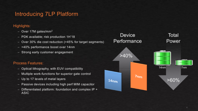
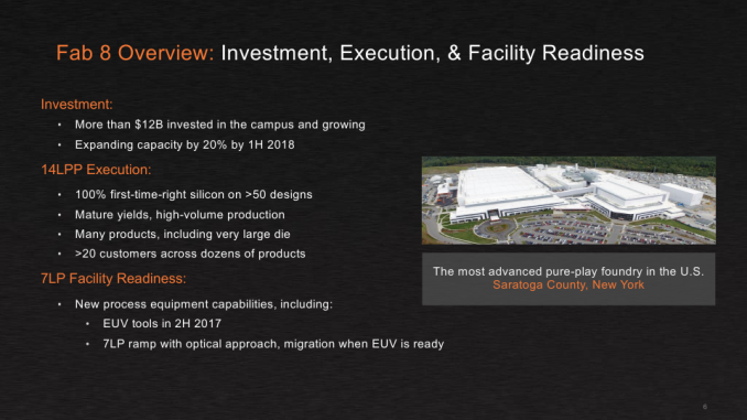
| 12:00p | GlobalFoundries Details 7 nm Plans: Three Generations, 700 mm², HVM in 2018 Keeping an eye on the ever-evolving world of silicon lithography, GlobalFoundries has recently disclosed additional details about its 7 nm generation of process technologies. As announced last September, the company is going to have multiple generations of 7 nm FinFET fabrication processes, including those using EUV. GlobalFoundries now tells us that its 7LP (7 nm leading performance) technology will extend to three generations and will enable its customers to build chips that are up to 700 mm² in size. Manufacturing of the first chips using their 7LP fabrication process will ramp up in the second half of 2018.
7 nm DUVFirst and foremost, GlobalFoundries reiterated their specs of their first-gen 7 nm process, which involves deep ultraviolet (DUV) lithography with argon fluoride (ArF) excimer lasers operating on a 193 nm wavelength. The company’s 7 nm fabrication process is projected to bring over a 40% frequency potential over the 14LPP manufacturing technology that GlobalFoundries uses today, assuming the same transistor count and power. The tech will also reduce the power consumption of ICs by 60% at the same frequency and complexity. For their newest node, the company is focusing on two ways to reduce power consumption of the chips: implementing superior gate control, and reducing voltages. To that end, chips made using GlobalFoundries' 7LP technology will support 0.65 – 1 V, which is lower than ICs produced using the company’s 14LPP fabrication process today. In addition, 7LP semiconductors will feature numerous work-functions for gate control.
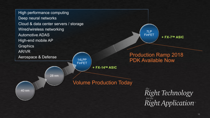
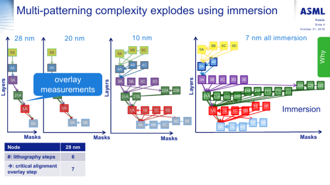
When it comes to costs and scaling, the gains from 7LP are expected to be a bit atypical from the usual manufacturing process node advancement. On the one hand, the 7 nm DUV will enable over 50% scaling over 14LPP, which is not something surprising given the fact that the latter uses 20 nm BEOL interconnections. However, since 7 nm DUV involves more layers that require triple and quadruple patterning, according to the foundry the actual die cost reduction will be in the range between 30% and 45% depending on application. The 7 nm platform of GlobalFoundries is called 7LP for a reason — the company is targeting primarily high-performance applications, not just SoCs for smartphones, which contrasts to TSMC’s approach to 7 nm. GlobalFoundries intends to produce a variety of chips using the tech, including CPUs for high-performance computing, GPUs, mobile SoCs, chips for aerospace and defense, as well as automotive applications. That said, in addition to improved transistor density (up to 17 million gates per mm2 for mainstream designs) and frequency potential, GlobalFoundries also expects to increase the maximum die size of 7LP chips to approximately 700 mm², up from the roughly 650 mm² limit for ICs the company is producing today. In fact, when it comes to the maximum die sizes of chips, there are certain tools-related limitations.
GlobalFoundries has been processing test wafers using 7 nm process technology for clients for several quarters now. The company’s customers are already working on chips that will be made using 7 nm DUV process technology, and the company intends to start risk production of such ICs early in 2018. Right now, the clients are using the 0.5 version of GlobalFoundries' 7 nm process design kit (PDK), and later this year the foundry will release PDK v. 0.9, which will be nearly final version of the kit. Keep in mind that large customers of GlobalFoundries (such as AMD) do not need the final version of the PDK to start development of their CPUs or GPUs for a given node, hence, when GF talks about plans to commercialize its 7LP manufacturing process, it means primarily early adopters — large fabless suppliers of semiconductors.
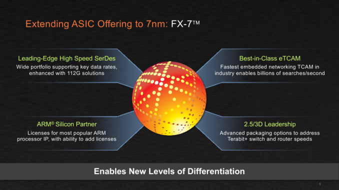
In addition to its PDKs, GlobalFoundries has a wide portfolio of licenses for ARM CPU IP, high-speed SerDes (including 112G), and 2.5D/3D packaging options for its 7LP platform. When it comes to large customers, GlobalFoundries is ready for commercial production of chips using its 7 nm DUV fabrication process in 2018.
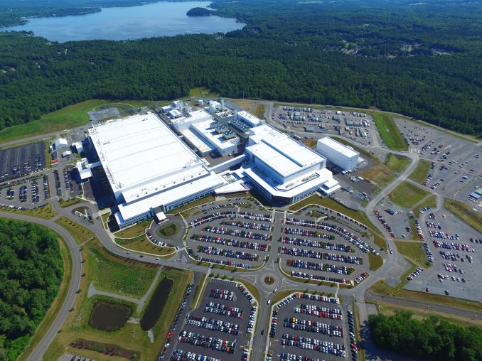
Fab 8 Ready for 7LP, Getting Ready for EUVSpeaking of high volume manufacturing using their 7LP DUV process, it is necessary to note that earlier this year GlobalFoundries announced plans to increase the production capacity of their Fab 8. Right now, the output of Fab 8 is around 60,000 wafer starts per month (WSPM), and the company expects to increase it by 20% for 14LPP process technology after the enhancements are complete.
The expansion does not involve physical enhancement of the building, which may indicate that the company intends to install more advanced scanners with increased output capabilities. GlobalFoundries naturally does not disclose details about the equipment it uses, but newer scanners with higher output and better overlay and focus performance will also play their role in HVM using 7 nm DUV that relies on quadruple patterning for select layers.
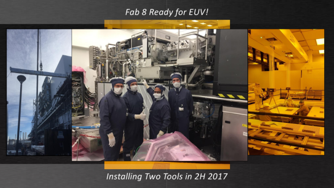
In addition to more advanced ASML TWINSCAN NXT DUV equipment, GlobalFoundries plans to install two TWNSCAN NXE EUV scanners into the Fab 8 in the second half of this year. This is actually a big deal because current-generation fabs were not built with EUV tools in mind. Meanwhile, EUV equipment takes up more space than DUV equipment because of the light source and other aspects.
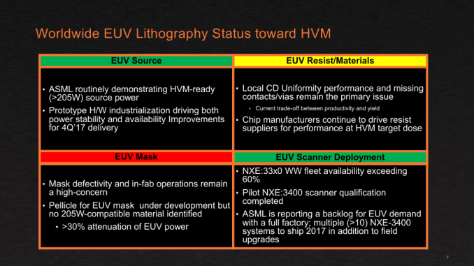
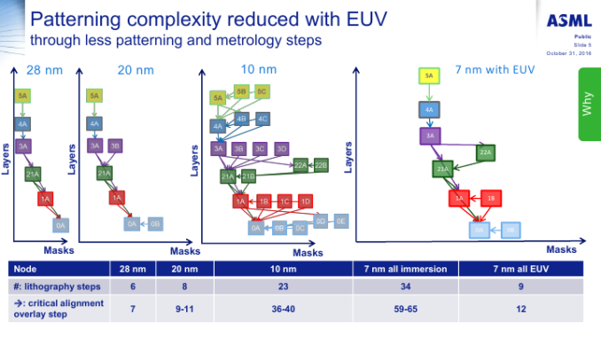
EUV: Many Problems Solved, By Concerns RemainUsage of multi patterning for ultra-thin process technologies is one of the reason why the industry needs lithography that uses extreme ultraviolet wavelength of 13.5 nm. As avid readers know, the industry has been struggling to develop EUV tools suitable for HVM, and while significant progress has been made recently, EUV is still not quite up to scale. This is exactly why GlobalFoundries is taking a cautious approach to EUV that involves multiple generations. Keep in mind that GlobalFoundries does not seem to have official names for different iterations of its 7 nm process technologies. The only thing that the company is talking about now is its “7LP platform with EUV compatibility.” Therefore, all our generations-related musings here are just for a better understanding of what to expect.
ASML has developed several generations of EUV scanners and has demonstrated light sources with 205 W of power. The latest TWINSCAN NXE scanners with recent upgrades have demonstrated an availability that exceeds 60%, which is good enough to start their deployment, according to GlobalFoundries. Eventually, availability is expected to increase to 90%, in line with DUV tools. Meanwhile, there are still concerns about protective pellicles (films) for EUV photomasks, mask defects, as well as EUV resists. On the one hand, current pellicles can handle productivity rates of up to 85 wafers per hour (WpH), which is well below 125 WpH planned for this year. Basically, this means that existing pellicles cannot handle powerful light sources required for HVM. Any defect on a pellicle can affect wafers and dramatically lower yields. Intel demonstrated pelliclized photomasks that could sustain over 200 wafer exposures, but we do not know when such pellicles are expected to enter mass production. On the other hand, powerful light sources are required for satisfactory line-edge roughness (LER) and local critical dimensions (CD) uniformity primarily because of imperfections of resists. 7 nm EUV Gen 1: Improving Yields, Reducing CyclesGiven all the EUV-related concerns, GlobalFoundries will start to insert EUV for select layers in a bid to reduce the usage of multi patterning (and eliminate quadruple patterning in general, if possible), thereby improving yields. At this time the company is not disclosing when it plans to start using EUV tools for manufacturing, only stating that they'll do so “when it is ready.” It is unlikely that EUV will be ready in 2018, so it is logical to expect the company to use EUV tools no sooner than 2019.
Such approach makes a lot of sense because it enables GlobalFoundries to increase yields for its customers and to learn more about what it will take to get EUV ready for HVM. In the best-case scenario, GlobalFoundries will be able to produce designs developed for 7 nm DUV with multi patterning using its 7 nm EUV tech. However, one should keep in mind two factors. First, semiconductor developers release new products every year. Second, GlobalFoundries will begin to insert EUV tools into production at least a couple of quarters after the launch of the first 7 nm DUV chips. Therefore, it is highly likely that the first EUV-based chips produced at GlobalFoundries will be new designs rather than chips originally fabbed on the all-DUV process.
7 nm EUV Gen 2: Higher Transistor Density and Line-Edge RoughnessDepending how fast the industry addresses the current EUV challenges related to masks, pellicles, CD uniformity, LER and other things, GlobalFoundries will eventually roll out another generation of its 7 nm EUV process. The second-gen 7 nm EUV manufacturing technology from GlobalFoundries will feature improved LER and a better resolution, which the company hopes will enable higher transistor densities with lower power and/or higher performance. Though given the experimental nature of the tech behind this process, as you'd expect GlobalFoundries is not saying when certain problems are to be resolved and when it can offer appropriate services to its customers. Finally, 3rd Gen 7LP will likely introduce some new design rules to enable geometry scaling and/or higher frequencies/lower power, but in general I'm expecting that the transition to this process should be relatively seamless to IC designers. After all, the majority of layers will still use DUV. The only question is whether GlobalFoundries will need to install additional TWINSCAN NXE scanners into the Fab 8 for its 2nd Gen 7 nm EUV process technologies, which would also indicate that the number of layers processed using EUV had increased. 5 nm EUV: Adjustable Gate-All-Around FETsA week before GlobalFoundries disclosed their 7LP platform plans, IBM and their Research Alliance partners (GlobalFoundries and Samsung) demonstrated a wafer processed using a 5 nm manufacturing process. ICs on the wafer were built using silicon nanosheet transistors (aka gate-all-around FETs [GAA FETs]) and it looks like they will be building blocks for semiconductors in the future. The big question of course is when.
GAA FETs developed by IBM, GlobalFoundries, and Samsung stack silicon nanosheets in such a way that every transistor now has four gates. The key thing about GAA FETs is that the width of nanosheets can be adjusted within a single manufacturing process or even within the IC design to fine-tune performance or power consumption. When it comes to performance/power/area(PPA)-related improvements, IBM claims that when compared to a 10 nm manufacturing process, the 5 nm technology offers 40% performance improvement at the same power and complexity, or 75% power savings at the same frequency and complexity. However keep in mind that while IBM participates in the Alliance, announcements by IBM do not reflect the actual process technologies developed by GlobalFoundries or Samsung.
IBM, GlobalFoundries, and Samsung claim that adjustments to GAA FETs were made using EUV, which is logical as the three companies use an ASML TWINSCAN NXE scanner at the SUNY Polytechnic Institute's NanoTech Complex (in Albany, NY) for their R&D work. Technically, it is possible to produce GAA FETs using DUV equipment (assuming that it is possible to get the right CD, LER, cycle times, etc.), but it remains to be seen how significantly the 5 nm process and designs will rely on EUV tools.
Neither of the three members of the Research Alliance talked about timeframe of 5 nm HVM, but a wild guess would put 5 nm EUV in 2021 (if not later).
Some ThoughtsWrapping things up, based on recent announcements it's looking increasingly likely that EUV will in fact make it out of the lab and intro high volume production. In just the past couple of weeks GlobalFoundries and two of its development partners have made several announcements regarding EUV in general, increasingly calling it a part of their future. This does not mean that they do not have a Plan B with multi patterning, but it looks like EUV is now a part of the mid-term future, not the long-term one. Still, it's telling that no one is giving a deadline for EUV beyond “when it is ready.”
Just like GlobalFoundries said before (like other foundries), the insertion of EUV equipment into their manufacturing flow would be gradual. The company plans to install two scanners this year to use them for mass production several quarters down the road, but GlobalFoundries has not made any further announcements beyond that. Ultimately while the future for EUV is looking brighter, the technology is still not ready for prime time, and for the moment no one knows quite when it'll finally meet all of the necessary metrics for volume production. Finally, speaking of the 7LP platform in general, it is interesting that GlobalFoundries will be primarily targeting high-performance applications with the new technology, and not mobile SoCs like some other contract fabs. This despite the fact that the 7LP platform supports ultra-low voltages (0.65 V) and should be able to address mobile applications. So from a performance/power/area point of view, while the 7LP manufacturing process looks rather competitive, it remains to be seen just how GlobalFoundries’ partners will use the capabilities of the new process. Related Reading: | ||||||||||||||||||||||||||||||||||||||||||||||||||||||||||||||||||||||||||||||||||||||||||||||||||||||||||||||||||||||||||||||||||||||||||||||||||||||||||||||||||||
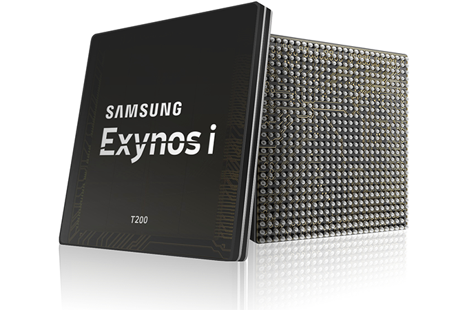
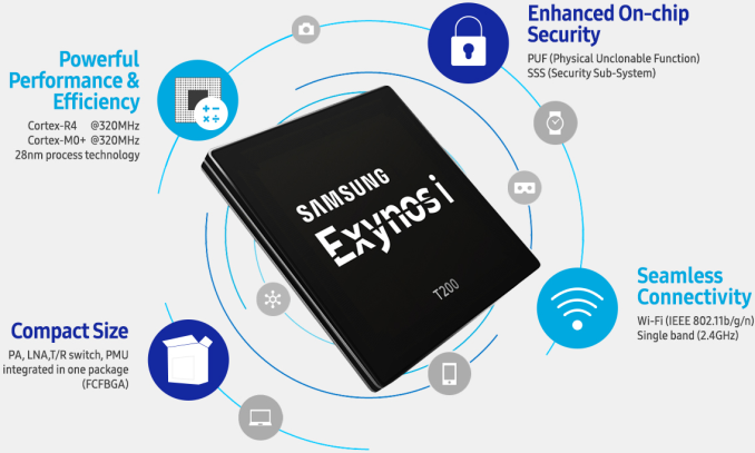
| 1:00p | Samsung Begins Production of Exynos i T200 SoC for Miniature IoT Devices
Samsung on Thursday said it had begun to mass-produce its first SoC for miniature IoT devices, the Exynos i T200. Aimed at devices that do not need a lot of compute power, but require ultra-low standby power consumption, the first Exynos i SoC integrates processing, connectivity, security and other capabilities. The Samsung Exynos i T200 SoC uses one ARM Cortex-R4 CPU core and one ARM Cortex-M0+ CPU core for real time processing and microcontroller applications, with both cores running at 320MHz. For connectivity, the chip also contains a 802.11 b/g/n single-band (2.4 GHz) Wi-Fi controller and supports IoTivity protocol that enables interoperability between IoT devices over various protocols. In addition, Samsung’s Exynos i SoC has a security hardware block called the Security Sub-System (SSS) as well as a physical unclonable function (PUF) for secure data storage and device authentication. The Exynos i T200 chip is made using Samsung’s “low power 28 nm HKMG” process technology, but Samsung does not specify which one. As for packaging, the SoC comes in an FCBGA form-factor.
Samsung did not indicate if and when it plans to start using the i T200 chip internally. Since Samsung also sells Exynos SoCs to third parties, it is possible that the Exynos i T200 ends up in devices made by other makers. As for pricing, the SoC uses a Cortex-R4 and a Cortex-M0+ cores, which are very small and optimized for low costs, therefore, it is unlikely that the Exynos i T200 will be expensive. Related Reading: | ||||||||||||||||||||||||||||||||||||||||||||||||||||||||||||||||||||||||||||||||||||||||||||||||||||||||||||||||||||||||||||||||||||||||||||||||||||||||||||||||||||


| << Previous Day |
2017/06/23 [Calendar] |
Next Day >> |