[Most Recent Entries] [Calendar View]
Wednesday, June 28th, 2017
- Micron Hires New CEO: Sanjay Mehrotra, SanDisk Co-Founder And Former CEO
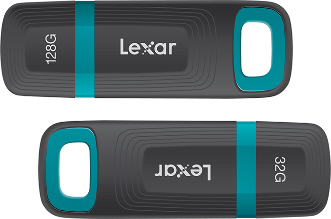
- Lexar Launches 'JumpDrive Tough' USB Drives up to 128GB: Focusing on Physical Endurance
- Micron Presents New SSDs and Strategy: From Components to Whole Solutions, 3D NAND Shipping Imminent
- Lexar Professional Workflow HR2 4-Bay Thunderbolt 2 / USB 3.0 Reader Hub Review
| Time | Event | ||||||||||||||||||||||||||||||||||||||||||||||||||
| 2:00a | Qualcomm Announces Snapdragon 450 Midrange SoC
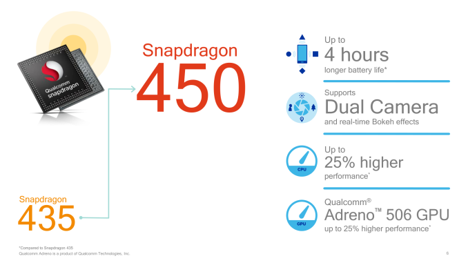
Kicking off today is second Mobile World Congress of the year, MWC Shanghai. As the de facto home of smartphone manufacturing, and home for an increasing number of major mobile device vendors, the tradeshow has taken on increased importance in recent years. This year is no exception, with several different announcements of note coming out of the show. Starting things off for everyone is Qualcomm, who is at the show to announce their latest mainstream Snapdragon 400 series SoC: the Snapdragon 450. The successor to Qualcomm’s 2016 Snapdragon 435, the Snapdragon 450’s biggest claim to fame is also its smallest: it will be the first Snapdragon 400 series SoC to be fabbed at 14nm, finally moving Qualcomm’s mainstream SoC lineup off of 28nm LP and on to a more recent and more power efficient manufacturing node.
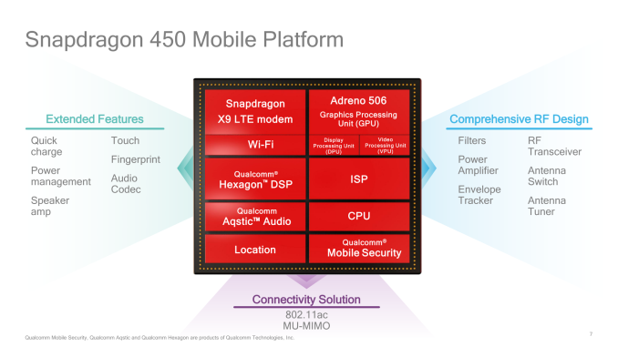
At a high level, the Snapdragon 450 is a very straightforward successor to the 435. Qualcomm has taken most of the 435’s design principles and brought them forward for the smaller Snapdragon 450. For example, we’re still looking at an octa-core ARM Cortex-A53 implementation, however thanks to the 14nm process Qualcomm has been able to bump up the maximum clockspeed from 1.4GHz to 1.8GHz. Similarly, Qualcomm has updated the GPU from an Adreno 505 on the Snapdragon 435 to an Adreno 506 on the Snapdragon 450, with the more powerful GPU said to offer 25% better performance.
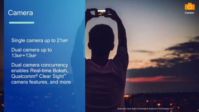
Meanwhile more significant upgrades have been made to the ISPs and USB controller. Similar to the Snapdragon 435, the 450 supports a single camera at up to 21MP. However if it’s used in a dual camera configuration – as is increasingly popular these days for artificial Bokeh and telephoto modes – then it can handle a pair of 13MP sensors, up from 8MP on the Snapdragon 435, and a notable improvement as 13MP seems to increasingly be the baseline for midrange phones. Qualcomm’s video processor blocks have also been improved, in part to keep up with the improved sensor, and as a result the 450 can now capture video at up to 1080p60, doubling the maximum framerate over the Snapdragon 435’s 1080p30 limit. Meanwhile the USB controller has been upgraded from USB 2.0 to USB 3.0, allowing for much faster transfers from Snapdragon 450 devices. And, like its predecessor, the 450 also supports QualComm’s QuickCharge 3.0 tech over said USB port.
Cellular connectivity is once again provided by Qualcomm’s Integrated X9 modem, which supports LTE Category 7 down and Category 13 up, for a maximum of 300Mbps down and 150Mbps up respectively. Interestingly, on the Snapdragon 435, Qualcomm limited that SoC for just 100Mbps up despite the fact that Category 13 allows for 150Mbps; so this is the first X9-equipped Snapdragon 400 SoC to actually be able to hit 150Mbps up, going by Qualcomm’s specifications. The 450 also retains the 435’s Hexagon DSP, however like so many other parts of the SoC, the 450’s DSP has been further enhanced to reduce power consumption. Last but not least, Qualcomm is promising some solid battery life improvements with the Snapdragon 450 over its 435 predecessor. While the company has invested some of their 14nm gains in improving clockspeeds throughout the chip, they’ve also retained a lot of those gains for reducing overall power consumption, a philosophy similar to what they did with the Snapdragon 835 this year as well. To that end the company is promoting that Snapdragon 450 phones will be able to deliver 4 hours more battery life relative to 435 phones.
Overall it’s interesting to note just how much the Snapdragon 450 sounds a lot like Qualcomm’s Snapdragon 625, their 14nm SoC from 2016. Both chips use a octa-A53 CPU configuration, X9 LTE modem, and Adreno 506 GPU. In fact the Snapdragon 450 is even pin compatible with the Snapdragon 625, which means that handset manufacturers can immediately begin working with the new SoC in existing designs. However given this close similarity, I’m also left to wonder whether the Snapdragon 450 is a new die, or a cut-down 625. In any case, the two chips still have some differences between them: particularly that the Snapdragon 625 clocks higher and features a more powerful ISP and video decode block. Wrapping things up, as is often the case with Qualcomm’s SoC reveals, today’s announcement comes ahead of vendor sampling and wide release. The company will begin commercial sampling in Q3 of this year, and the chip should show up in retail devices by the end of the year. Gallery: Qualcomm Snapdragon 450 Press Deck
      | ||||||||||||||||||||||||||||||||||||||||||||||||||
| 6:00a | Qualcomm Announces Snapdragon Wear 1200 SoC: LTE Categories M1 & NB1 for Wearables & Smart Trackers
Back around this time last year, Qualcomm introduced their Snapdragon Wear 1100, the company’s first SoC specifically designed for budget, low-power wearable devices. The humble SoC featured just a single Cortex-A7 CPU core and LTE Cat 1 support, but for the market Qualcomm had designed it for, this was more than sufficient. Now at MWC Shanghai 2017, the company is launching an even more low power successor to the Snapdragon Wear 1100, the aptly named Snapdragon Wear 1200. The Snapdragon Wear 1200 is an interesting development from Qualcomm, as while the name can be a bit deceiving, it’s the first in a new generation of products for the company. Taking the basic principles of the 1100, Qualcomm has integrated a new modem that supports new, ultra-low-power communication modes for LTE standardized in the last year: LTE Category M1 and Category NB1. In fact this is Qualcomm’s first SoC to support the 3GPP’s Low Power WAN technologies.
Briefly touching on the specs of the Wear 1200, the core processor is almost unchanged from the Wear 1100. The SoC is still powered by a single Cortex-A7 CPU core and paired with a simple display controller that is just barely a fixed function GPU. It is meant to be a low-power (and low cost) SoC, through and through. The big change here for Qualcomm is on the modem side. Whereas the Wear 1100 shipped with a multi-mode 2G /3G / LTE Cat 1 modem – as low a power a design as one could get at the time – the Wear 1200 incorporates a much more power-efficient and very much forward-looking modem. One that supports only basic 2G (E-GPRS) functionality, along with the aforementioned LTE Cat M1 and NB1 standards. This is the first product announcement to cross our desk supporting these new standards, and ultimately the Snapdragon Wear 1200 will be the first of many devices/chips that we see to do so. Part of the 3GPP’s Release 13, the standards body has been focusing on reducing power consumption, complexity, and costs for radios for IoT devices, wearables, and other simple devices as part of their LPWAN initiative. At a high level, LTE Cat M1 is designed to be a relatively straightforward, further power-optimized form of LTE. The max data rate is just 1Mbps up and down – and the Wear 1200 doesn’t even reach those speeds – using tricks like a minimum-width 1.08Mhz channel and half-duplex communication to cut power consumption, all the while still being compatible with existing LTE networks. LTE Cat NB1 takes this a step further, going with a stand-alone LTE-derived narrowband implementation that uses just a 180KHz channel, which combined with other technologies offers the lowest amount of bandwidth (max 250Kbps) but also the lowest power consumption and improved range.
For Qualcomm and other wearable/IoT device manufacturers, these new standards will be a significant part of making the Internet of Things live up to its name, by allowing even the lowest-power, lowest-cost devices to have LTE network functionality. Unsurprisingly then, one of the first places we’re going to see it deployed is in low-cost wearables, where Internet access is beneficial, but battery life concerns are significant. As for the Wear 1200 in particular, Qualcomm’s wearable-class SoC keeps a low profile even for M1/NB1 devices. The SoC can support 300Kbps down and 375Kbps up for Cat M1, and just 20Kbps down and 60Kbps up for Cat NB1. And no, the latter isn’t a typo: NB1 devices are expected to send data as much (if not more than) they receive it, so the Wear 1200’s data rates vary accordingly. Meanwhile, despite the limited bandwidth these standards offer, the Wear 1200 supports 15 RF bands along with some notable LTE features, particularly VoLTE. Interestingly however, while Qualcomm supports the latest low-power IoT standards, they don’t support the equivalent low-power 2G standard, EC-GSM. The Wear 1200 does support 2G in the form of E-GPRS, so there is GSM backwards compatibility for when LTE isn’t available, but the future Qualcomm is planning for is very much one where LTE is everywhere and 2G won’t be needed. Modems aside, the Wear 1200 is otherwise a function-optimized design. Like its predecessor, the SoC supports WiFi and Bluetooth for various connectivity options, along with augmenting the standard GPS/GLONASS/Beidou/Galileo geo positioning systems. The new SoC retains the same small size of its predecessor, with the chip measuring 79mm2. Overall, Qualcomm is touting a 10 day standby battery life for the SoC, which would be a significant improvement over the 7 day standby of the Wear 1100. Finally, looking at the broader picture, the wearables market is still trying to figure out what it wants to be – and what consumers will actually buy – and for the Wear 1200 Qualcomm is particularly interested in courting the “kid watch” market. A segment of the larger smart tracker market, Qualcomm is looking to tap into what is already a significant market in Asia – and especially China – where it’s not uncommon to give your kid a limited functionality watch that allows you to contact them, while the watch works in conjunction with geofencing applications to keep tabs on their whereabouts. Driven in part by demographics and in part by technology, Qualcomm expects the market for kid tracking watches to further grow, with SoCs like the Wear 1200 further improving the utility of these devices and bringing their cost down. These improvements would also filter down to other parts of the smart tracker market, such as pet tracking and elderly tracking devices. In fact the company is hitting the ground running: along with the launch of today’s SoC, they are also partnering with Borqs and Quanta to develop smart tracker/kid watch reference designs, so that hardware manufacturers can get a jump on developing Wear 1200-based trackers. And like the Snapdragon Wear 1200 itself, these reference designs are available and shipping today. So while Qualcomm isn’t specifically commenting on when their customers’ consumer devices will be ready, it will almost certainly be before the end of the year. | ||||||||||||||||||||||||||||||||||||||||||||||||||
| 8:00a | Western Digital My Passport SSD Mini-Review Flash-based external direct-attached storage (DAS) devices have evolved rapidly over the last few years. Starting with simple thumb drives that could barely saturate USB 2.0 bandwidth, we now see high-performance external SSDs. The full performance from these new crop of external storage devices can only be realized using the USB 3.1 Gen 2 interface. Western Digital's My Passport SSD is an external SSD with a USB 3.1 Gen 2 Type-C interface. It caters to the mainstream market and comes in three capacities - 256GB, 512GB, and 1TB.In this review, we take a look at the 1TB version. | ||||||||||||||||||||||||||||||||||||||||||||||||||
| 10:00a | Western Digital Announce BiCS4 3D NAND: 96 Layers, TLC & QLC, Up to 1 Tb per Chip
Western Digital on Tuesday formally announced its fourth-generation 3D NAND memory, developed as part of the Western Digital/Toshiba joint venture. The fourth-generation BiCS NAND flash chips from Western Digital feature 96 layers and will include several capacity points and will use TLC and QLC architectures. The company expects to start volume production of BiCS4 chips in 2018. NAND dies that belong to the fourth-generation BiCS 3D NAND will use 96 word layers to minimize die size of the chips and maximize output of fabs, and at this point represents the largest layer count in the flash memory industry. Furthermore the range of BiCS4 NAND die configurations available will be considerably more diverse than BiCS3, which currently only includes 256 Gb and 512 Gb dies. Western Digital plans to offer BiCS4 components based on TLC (triple level cell) and QLC (quadruple level cell) configurations. with capacities ranging from 256 Gb to 1 Tb. It is noteworthy that Western Digital’s BiCS4 lineup will include QLC NAND, which has been discussed by Western Digital (and SanDisk before that) for several years, but which is about to become reality only in the coming quarters. To store four bits per cell (with 16 voltage states) Western Digital had to use a “thick” process technology alongside multi-layer 3D NAND to keep the per-bit costs down. The company is not specifying how many program/erase cycles its 3D QLC NAND will handle, but various industry predictions over the years have suggested 100 – 150 P/E cycles as a reasonable goal for QLC NAND, which is considerably lower than approximately 1000 P/E cycles supported by TLC NAND. Given such endurance, it is logical to expect 3D QLC NAND to be used for primarily removable storage as well as for ultra-high capacity datacenter drives for the so-called near-WORM (write once read many) storage applications. For example, Toshiba last year discussed a QLC-based datacenter SSD with 100 TB capacity for WORM apps.
Western Digital plans to begin sampling of select 96-layer BiCS4 3D NAND configurations in the second half of this year, but the manufacturer does not specify which dies will sample when. As for mass production, Western Digital intends to start volume manufacturing of their 96-layer 256 Gb 3D NAND in 2018, with other dies to follow later. Based on Western Digital’s announcements made earlier, the company will gradually introduce more sophisticated BiCS4 96-layer configurations in 2018 and 2019, before moving to BiCS5 sometimes in 2020. That said, it makes sense to expect the highest capacity BiCS4 ICs to ship later rather than sooner.
Finally, Western Digital did not disclose whether it uses NAND string stacking technology to assemble its 96-layer 3D NAND dies, but it is a likely scenario given what industrial publications have been predicting. Related Reading: | ||||||||||||||||||||||||||||||||||||||||||||||||||
| 9:00p | Micron Discontinues Lexar Business, Plans to Focus on Higher-Margin Products
Micron this week announced plans to discontinue its Lexar removable media storage business as a part of the company’s strategy to shift to higher margin NAND flash-based products. The company intends to sell all or part of its Lexar business division, but promises to support existing customers during the transition period. Lexar was spun off from Cirrus Logic in 1996 and then acquired by Micron in 2006 in a bid to market NAND flash media. More recently, approximately two years ago, Micron cut down the amount of NAND memory it supplied to spot market in a bid to concentrate on building its own products and thus earn higher profit margins. Last year the company announced plans to work with its clients to build software for their software storage offerings to further improve its profit margins, this time from various SSDs. In addition, the company disclosed plans to develop special memory solutions for emerging automotive applications (which will complement its embedded portfolio). This week Micron went even further and disclosed plans to cease selling Lexar branded products to consumers and OEMs as a part of its strategy to increase “opportunities in higher value markets and channels.” The portfolio of Lexar products includes memory cards and card readers, USB flash drives and even SSDs. Given the competition on the market of retail removable media and storage drives, the withdrawal from such businesses may be logical for Micron, which feels increasing pressure from Samsung, Western Digital (SanDisk) and others amid lack of market growth in terms of NAND bits (at least, according to its own predictions). Meanwhile, the withdrawal also means that Micron will have to concentrate on production of SSD-grade memory, whereas any further removable storage-grade NAND that the company produces will have be sold on the open market. If someone buys the Lexar operations from Micron, the latter will likely sign some kind of exclusive supply agreement with the new owner, which means that it will keep developing the aforementioned NAND. SSD-grade memory is more expensive than chips for memory cards or USB flash drives. and for about a year Micron was the only company to sell its SSD-grade 3D NAND to third-party SSD vendors, possibly earning higher margins than by selling removable storage devices. However, NAND for the latter is typically used to test drive new production technologies and/or architectures before deploying them to make memory for SSDs.
Otherwise, looking at the bigger picture, Micron new alignment with regards to the removable storage market is not particularly unique. SK Hynix and Intel don't produce removable storage products either (at least, not under their own trademarks), leaving Samsung, Toshiba and Western Digital as the three remaining vendors who do. That said, while it will be sad to see Micron’s Lexar gone (assuming that nobody buys it), Micron’s withdrawal from removable storage business is not exactly surprising. Related Reading: | ||||||||||||||||||||||||||||||||||||||||||||||||||


| << Previous Day |
2017/06/28 [Calendar] |
Next Day >> |