[Most Recent Entries] [Calendar View]
Tuesday, August 15th, 2017
- The AMD Zen and Ryzen 7 Review: A Deep Dive on 1800X, 1700X, and 1700
- The AMD Ryzen Threadripper 1950X and 1920X Review: CPUs on Steroids
- The Intel Skylake-X Review: Core i9 7900X, i7 7820X, and i7 7800X Tested
- AMD Announces Ryzen AGESA 1.0.0.65 Update: Enables Memory Clocks Up To DDR4-4000
- Patriot Publishes List of AMD Ryzen Compatible DIMMs: Up to DDR4-3400, 64GB
- EUV Lithography Makes Good Progress, Still Not Ready for Prime Time
- Samsung and TSMC Roadmaps: 8 and 6 nm Added, Looking at 22ULP and 12FFC
- GlobalFoundries Updates Roadmap: 7 nm in 2H 2018, EUV Sooner Than Later?
| Time | Event | ||||||||||||||||||||||||||||||||||||||||||||||||||||||||
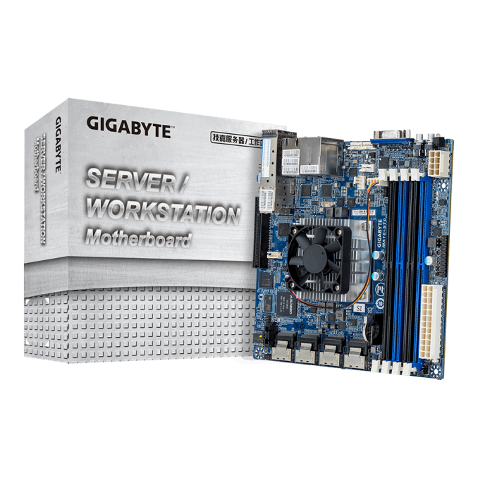
| 3:33a | More Denverton Noise: GIGABYTE’s MA10-ST0 Features Unannounced 16-Core C3958
Today GIGABYTE Server (the server arm of GIGABYTE, a different BU to the motherboard team) has lifted the lid on their new MA10-ST0 motherboard and SoC combination, aimed squarely at the cold storage or edge storage market. This includes base support for up to 16 SATA drives via SFF8087, a PCIe x8 slot, 10 gigabit Ethernet via two SFP+ ports, and server management features via the Aspeed AST2400. For server/enterprise features, a TPM header and a COM header are also present. The interesting twist in this tale, however, is the SoC at the heart of the unit.
GIGABYTE Server has announced they are using the C3958 SoC, listed as a 16-core part at 31W TDP and supporting DDR4-2400. The C3000 series is known as the Denverton family of CPUs, based on Intel’s Goldmont Atom microarchitecture. The Denverton CPU family has been formally announced, although only as a single SKU, the dual core C3338, which is present in some enterprise NAS devices. Some others have cited cloud instances featuring unannounced Denverton CPUs being deployed and available by cloud providers. This C3958 is another unannounced processor from Intel.
Intel’s Atom line in this market is still recovering from the Avoton/Rangeley issue that cropped up 18-24 months after launch, which had an outside chance of burning out the signal generator resulting in a system that would be unable to be repaired (we are told that an unusual spike in failures is not expected from this, but for users who deploy 10-15 year embedded devices it might be in the back of their minds). From this, Intel released a new stepping of the CPU to address the bug, and some have predicted that the delays to the formal announcement and release of the Denverton stack (some 12 months or more after the expected announcement date) is due to ensuring Denverton does not have this issue. As for the C3958, GIGABYTE Server lists this as Intel’s top Denverton SoC model, running at 16 cores, 1MB of L2 per core, 2.0 GHz base frequency (no word on turbo), support for up to 128GB of DDR4-2400 RDIMMs (or 64GB of UDIMMs, i.e. 4x16GB modules) and having a 31W TDP. Typically around this SoC level, we might expect to compare it to an E3-1200 v6 series processor, although those CPUs start at 72W. The previous generation Rangeley processor topped out at 8 cores and 2.4 GHz for 20W, so on paper there looks to be some efficiency gain despite the frequency decrease. As for the MA10-ST0 motherboard, along with all the features above it also comes with 32GB of eMMC flash, allowing a user to install a storage-based OS for a network deployment without using any of the onboard SATA ports. GIGABYTE Server has told us that board is essentially ready to go, and interested parties should get in contact with their local reps. Related Reading | ||||||||||||||||||||||||||||||||||||||||||||||||||||||||
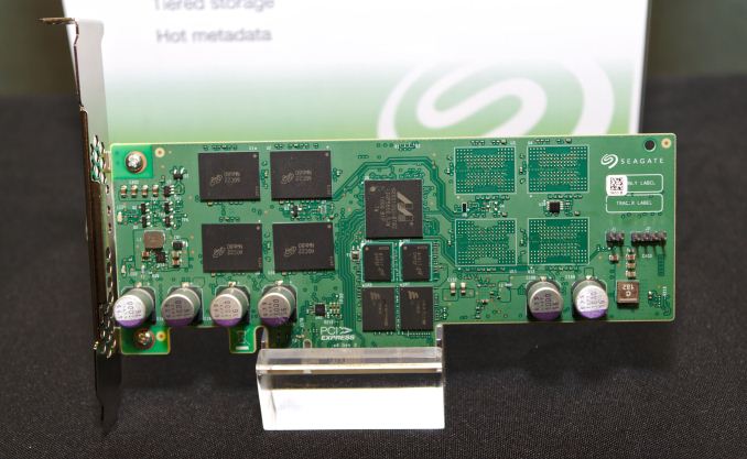
| 8:30a | Seagate Demos New SSD Features And Prototypes At FMS
In spite of a fire that closed the exhibition floor last week at Flash Memory Summit, Seagate managed to set up several live demos and display their latest SSDs along with a few prototypes, all in a meeting room safely away from the ruined exhibits. We've previously covered the new products Seagate announced at the beginning of the show last week. Pictures of the Nytro 5000 M.2 SSD, the 15TB Nytro 3000 series SAS SSD, and the 64TB demo based on eight M.2 SSDs are all in the gallery below. Live DemosThe two live demos used what appeared to be Nytro XP7102 SSDs in the half-height half-length add-in card form factor, but with Micron 3D NAND instead of the planar MLC that the XP7102 launched with. These drives use the same Marvell 88SS1093 controller that is in the Nytro 5000 and in several consumer SSDs. The live demos showed that Seagate has implemented support for the Streams feature from the NVMe 1.3 specification, and IO determinism which has been approved for the next revision of the NVMe specification.
The Streams demo illustrated how tagging write operations according to which task they belong to allows the SSD to keep related writes together and put unrelated data in separate erase blocks. When used properly, data from the same stream can be expected to have a similar lifetime, so when part of it gets invalidated or overwritten, everything in that erase block will also soon be available for garbage collection. With the longer-lived data stored elsewhere, the SSD has far less data to move and compact during its garbage collection process, which leads to lower write amplification and improved performance. For the test scenario Seagate concocted, they were able to show write amplification being reduced from around 8.6-9 down to about 1.03, while throughput for the worker thread that was shown on screen improved from around 9.7k IOPS to 83k IOPS. The new NVMe IO Determinism feature serves a similar purpose, but implements it in a very different way. NVMe Streams directives are essentially hints to the SSD controller about how to physically organize data. The IO Determinism feature asks the SSD to make hard guarantees by dividing its flash chips and channels into separate NVM Sets. IO to one set will never block access to another set because the data resides on different physical chips. Saturating the PCIe link or overloading the controller's available CPU power would be the only ways for one task to degrade another's IO performance. The downside to this static partitioning method is that a single task accessing one NVM Set will not be able to use the full performance or capacity of the drive, even if there are no other tasks accessing the drive.
The IO Determinism feature also provides for timeslicing access to the SSD, where the drive can provide a window for deterministic IO where background garbage collection is suspended, followed by a non-deterministic period where normal access is permitted by performance may be degraded as the garbage collector catches up. This is essentially a standardization of the "Host Managed SSD" feature OCZ implemented for its Saber 1000 enterprise SATA SSDs in 2015. PrototypesSeagate also showed off two unannounced prototypes that they had not planned to feature at their booth. The first was dubbed the Nytron 5000B, a variant of the Nytro 5000 M.2 SSD that is intended as a high-performance boot drive. This was commissioned by a large customer that did not wish to be named. The drive included 256GB of 3D MLC NAND and 2GB of DRAM, plus a connection to an external pack of capacitors. With such a large bank of capacitors, the 5000B can be far more aggressive about caching both metadata and user data in DRAM, allowing for burst write performance far in excess of what the flash could sustain, and without compromising data safety.
The other prototype had similar aims, but instead of a capacitor-backed bank of DRAM it featured 128MB of Everspin STT-MRAM in addition to a normal DRAM cache for metadata. Seagate envisions using the MRAM either as a write cache for user data, or exposing it directly as a separate storage namespace for explicit tiered storage. This MRAM prototype drive was not a preview of an upcoming product. Instead, Seagate views this as a test platform to explore the possibilities and performance characteristics of MRAM, now that it is available in useful capacities.
Gallery: Seagate Demos at FMS 2017
      | ||||||||||||||||||||||||||||||||||||||||||||||||||||||||
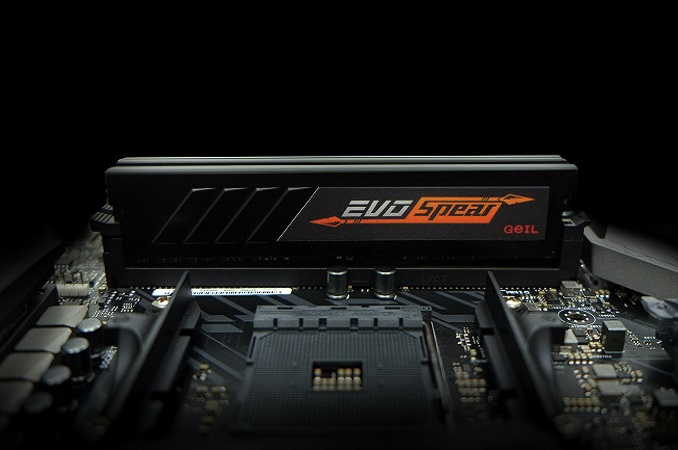
| 8:30a | Geil Announces EVO Spear Series DRAM: Up to DDR4-3466
Geil recently announced the availability of its new EVO Spear series of memory, with kits labeled specifically for either Intel and AMD Ryzen based systems. Geil states the EVO Spear series is intended for gamers, enthusiasts, and case modders looking for a cost-effective upgrade. The two flavors give one for Intel and the other for AMD Ryzen with capacities up to 64GB and speeds reaching 3600 MT/s (although not at the same time). Geil says the EVO Spear series of RAM is optimized for Intel Core X, i7, and i5 Processors which includes the Z200 and X299 series chipsets. They go on to say the AMD Edition sticks are fully compatible with Ryzen 7, Ryzen 5 Processors, and AM4 motherboards, and we suspect that Ryzen 3 and Threadripper will be supported eventually as well. The only differences between the two versions are the QVL and compatibility testing - while most kits should work in most boards, the AMD kits are officially certified in various AM4 boards and Intel kits for 200-series boards. The maximum speed on the AMD Edition kits top out a bit lower as well. From Ryzen's release day, board partners have been working with AMD to further increase compatibility with AGESA updates via new BIOS, and the market is seeing more and more AMD compatible RAM at faster speeds as time goes on, so the updates are working. The AMD Edition sticks have an AMD Ryzen logo found on the packaging and modules, while the Intel sticks are nondescript.
Capacities range from 16GB up to 64GB in both dual and quad channel kits. The operating frequency for the Intel sets is up to 3466 MHz, while the AMD Edition peaks at 3200 MHz. CAS ratings will vary by SKU but range from CL15 to CL17m and Geil offers a limited lifetime warranty on the EVO Spear Gaming Memory. The DIMMs use standard height heat sinks ensuring “zero mechanical interference” from the sticks. They are available only in a stealth black heat colored spreader with the EVO Spear name on the side. The heat spreader covers a black PCB, and in an effort to remain cost effective, RGB LEDs are not on the EVO Spear line.
In total there are over 50 different kits coming to market, divided by capacity (2x4 GB, 2x8 GB, 2x16 GB, 4x4GB, 4x8GB, 4x16GB) - the Geil website has the details. Pricing was not listed, however, a couple of dual channel kits are already available on newegg.com. A 2x8GB DDR4-2400 CL16-16-16-36 AMD Edition kit sells for $130.99 and a 2x8GB DDR4-2800 CL16-16-16-36 kit is asking $135.99. Related Reading: | ||||||||||||||||||||||||||||||||||||||||||||||||||||||||
| 9:20a | Intel Officially Reveals Post-8th Generation Core Architecture Code Name: Ice Lake, Built on 10nm+
In an unusual move for Intel, the chip giant has ever so slightly taken the wraps off of one of their future generation Core architectures. Basic information on the Ice Lake architecture has been published over on Intel's codename decoder, officially confirming for the first time the existence of the architecture and that it will be made on Intel's 10nm+ process. The Ice Lake processor family is a successor to the 8th generation Intel® Core™ processor family. These processors utilize Intel’s industry-leading 10 nm+ process technology.
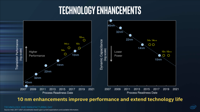
This is an unexpected development as the company has yet to formally detail (let alone launch) the first 10nm Core architecture – Cannon Lake – and it's rare these days for Intel to talk more than a generation ahead in CPU architectures. Equally as interesting is the fact that Intel is calling Ice Lake the successor to their upcoming 8th generation Coffee Lake processors, which codename bingo aside, throws some confusion on where the 14nm Coffee Lake and 10nm Cannon Lake will eventually stand. As a refresher, the last few generations of Core have been Sandy Bridge, Ivy Bridge, Broadwell, Haswell, Skylake, with Kaby Lake being the latest and was recently released at the top of the year. Kaby Lake is Intel’s third Core product produced using a 14nm lithography process, specifically the second-generation ’14 PLUS’ (or 14+) version of Intel's 14nm process. Meanwhile when it comes to future products, back at CES Intel briefly showed a device based on post-Kaby Lake designs, called Cannon Lake and based on their 10nm process. Since then Intel has also confirmed that the 8th Generation of processors for desktops, called Coffee Lake, will be announced on August 21st (and we recently received promotional material to that effect). Ice Lake then, seems poised to follow both Coffee Lake and Cannon Lake, succeeding both architectures with a single architecture based on 10nm+. Working purely on lithographic nomenclature, Intel has three processes on 14nm: 14, 14+, and 14++. As shown to everyone at Intel’s Technology Manufacturing Day a couple of months ago, these will be followed by a trio of 10nm processes: 10nm, 10nm+ (10+), and 10++,
On the desktop, Core processors will go from 14 to 14+ to 14++, such that we move from Skylake to Kaby Lake to Coffee Lake. On the Laptop side, this goes from 14 to 14+ to 14++/10, such that we move from Skylake to Kaby Lake to Coffee Lake like the desktops, but also that at some time during the Coffee Lake generation, Cannon Lake will also be launched for laptops. The next node for both after this is 10+, which will be helmed by the Ice Lake architecture.
The way that the desktop and laptop markets will be diverging then converging is confusing a lot of people. Why is the laptop market splitting between 14++ and 10, and why is the desktop market not going to 10nm but straight to 10+? What lies beyond is a miasma of guess work, leaked slides, and guessing Intel’s strategy, but I believe the answer lies in Intel’s manufacturing technologies and the ability to move to newer lithographic nodes. (We should interject here that the naming of a lithographic node has slowly lost its relevance between the features of the process and the actual transistor density and performance, such that TSMC’s improved 16FF+ is called 12FFN, but relies on similar transistor sizes with enhanced attributes. But 12 is a smaller number than 14, which is the marketing angle kicking in. By all accounts, Intel has typically been considered the more accurate foundry when it comes to numerical lithographic naming of the process, which others consider is to their detriment.) Intel originally predicted that they would move to 10nm almost a year ago, at the end of 2016 and 2 years after the launch of their 14nm process. But the challenge in managing the technology required to advance to their version of 10nm has been fraught with difficulty. In all cases it can depend on external equipment, fine tuning a process, or getting acceptable yields – while one manufacturer might be satisfied with an 80% yield, another might consider that a failure. Being able to obtain high yields (ramp up) will also be a function of die size, and so the newest nodes are typically launched with smaller mobile parts in mind first, as the yields for smaller parts are better than larger parts at the same defect rate. Simply put, the first generation of 10nm requires small processors to ensure high yields. Intel seems to be putting the smaller die sizes (i.e. anything under 15W for a laptop) into the 10nm Cannon Lake bucket, while the larger 35W+ chips will be on 14++ Coffee Lake, a tried and tested sub-node for larger CPUs. While the desktop sits on 14++ for a bit longer, it gives time for Intel to further develop their 10nm fabrication abilities, leading to their 10+ process for larger chips by working their other large chip segments (FPGA, MIC) first. From a manufacturing standpoint, Intel has been using multiple patterning techniques in its 14nm processes, and the industry is looking to when the transition to EUV will take place. Anton has some great writeups of the state of EUV and how different companies are transitioning to smaller nodes - they are well worth a read. The crux of the matter is that EUV would shorten time to market and arguably make the process easier (if only more expensive), and several fab companies are waiting for Intel to jump onto it first. With EUV not ready, Intel has had to invest into deeper multi-patterning techniques, which raise costs, decrease yields, and increase wafer process times considerably. All of which leads to a miasma of increased delays, much to the potential chagrin of investors but also customers who had banked on the power improvements that a typical new lithography node brings. Intel is still keeping spirits high, by producing numbers that would suggest that their methodology is still in tune with Moore’s Law, even if the products seem to be further strung out. Some analysts concur with Intel’s statements, while others see it as hand-waving until 10/10+ hits the market. Intel would also point out that it is developing other technologies such as Embedded Multi-Die Interconnect Bridges (EMIB) to assist in equipping chip with high-speed fabric or glue-logic.
Given its position as a post-8th gen architecture, Ice Lake is likely to hit sometime in 2018, perhaps 2019, depending on Intel’s rate of progress with larger chips and the 10+ process. Intel’s other market segments, such as FPGAs (Altera), Xeon Phi (MIC) and custom foundry partners, are also in the mix to get into some 10nm action. (Note that Intel’s next generation of Xeon Scalable Processors is called Cascade Lake, a 2018 refresh of the Skylake generation launched this year.) Gallery: Intel Manufacturing Tech Day
      | ||||||||||||||||||||||||||||||||||||||||||||||||||||||||
| 10:00a | Samsung Portable SSD T5 Review: 64-Layer V-NAND Debuts in Retail Samsung has been an active participant in the high-performance external SSD market with their Portable SSD series. The T1 was introduced in early 2015, while the T3 came out in early 2016. The T3 was the first retail product to utilize Samsung's 48-layer TLC V-NAND. Today, Samsung is launching the Portable SSD T5. It is a retail pilot vehicle for their 64-layer TLC V-NAND as they ramp up its production. The Portable SSD T5 also moves up to a USB 3.1 Gen 2 Type-C interface, while retaining the same compact form factor and hardware encryption capabilities of the Portable SSD T3. Read on for our analysis of the product's performance and value proposition. | ||||||||||||||||||||||||||||||||||||||||||||||||||||||||


| << Previous Day |
2017/08/15 [Calendar] |
Next Day >> |