[Most Recent Entries] [Calendar View]
Monday, August 28th, 2017
| Time | Event | |||||||||||||||||||||||||||||||||||||||||||||||||||||||||||||||||||||||||||||||||||||||||||||||||||||||||||||||||||||||||||
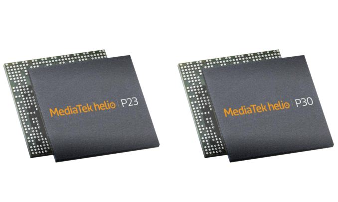
| 9:30a | MediaTek Unveils Helio P23 & Helio P30 SoCs: Premium Midrange for Q4'17 & Beyond
This morning MediaTek is taking the wraps off of their latest SoCs for the midrange phone market. Dubbed the Helio P30 and Helio P23, these are robust upgrades to the P20 series launched over the last year and a half, retaining the same octa-core Cortex-A53 CPU architecture but upgrading many other facets of the SoCs, including the GPUs and modems. MediaTek will be rolling these out next quarter, with the P23 going worldwide while the P30 starts its life in China. MediaTek is of course one of the industry’s most prolific SoC vendors, and these days one of a handful of independent smartphone SoC vendors not directly tied to a handset vendor. As a result their chips tend to show up frequently in the GSM/LTE market, especially in the midrange market where they have made a name for themselves. The Helio P-series is the company’s bread and butter in this space, targeted at what the company calls the “Premium Performance” market – calling for still price-conscious SoC designs that incorporate typical midrange core processor blocks (e.g. Cortex-A53) but pair that with higher-end ancillary features.
For SoC vendors like MediaTek, the midrange market has long been considered a good mix of volume and profitability – a growing user base that can afford something better than bare-featured (and cut-throat priced) low-end SoCs. It’s also one that MediaTek expects is going to continue to grow as carrier and government subsidies fade away and consumers have to bear the full cost of the phone. Moving on to the hardware itself, the Helio P30 and P23 are the follow-ups to the Helio P25 and P20, which were launched in February of 2017 and 2016 respectively. Essentially the same design for both SoCs, the P25 added a clockspeed bump as a mid generation upgrade for the family, offering better performance with the same feature set. The new P30 and P23, on the other hand, are more robust upgrades for the family, and while they’re not entirely detached from the P20 series parts we’ve seen so far, they incorporate new features and newer generation IP blocks to bring the family closer to the more recently launched Helio X30.
Relative to the P20/P25, the core CPU configuration has not changed. MediaTek is still using an octa-core Cortex-A53 setup, composed of two quad-core clusters. On both SoCs the performance cluster is clocked at 2.3GHz, while the efficiency cluster is clocked at 1.65GHz. Relative to the P25, this is actually a bit of a pullback in terms of the performance cluster clockspeed – from 2.6GHz to 2.3GHz – while the efficiency cluster is slightly faster. The Cortex-A53 is the tried and true workhorse of the midrange market due to its small size and low power consumption, and while its successor will come in the form of the Cortex A55, MediaTek’s new SoCs are a bit too early to integrate it. Instead, it looks like the CPU performance of these new P-series SoCs will be fairly close to the P20 and P25. However outside of the CPU clusters, almost every other part of the SoC has been updated for the P23 and P30. On the GPU side, for example, MediaTek is moving from ARM’s last-generation Mali T880 design to their current-generation Mali-G71 GPU. Based on ARM’s Bifrost GPU architecture, the Mali-G series is a major overhaul in how the company designs their GPUs. MediaTek is using a G71MP2 configuration in both SoCs, similar to the use of a T880MP2 configuration in the last-generation parts, with the P23’s GPU clocked at 770MHz, while the P30 will be clocked at a significantly higher 950MHz. Given both the architecture and the clockspeed differences, it will be interesting to see how the new Helio P-series SoCs compare to the existing P20 parts. However if you want to get into the upgrades and enhancements that MediaTek considers most important, it’s video capture, cameras, and their LTE modem.
With regards to video capture, MediaTek has also upgraded the video encode and decode blocks, but only the P30 gets outright new functionality. The P23 retains the same 4Kp30 H.264 recoding capabilities as its predecessor, along with 4Kp30 H.264 and HEVC decoding. The P30 takes things up a notch, adding HEVC to its encoding capabilities. Meanwhile on the camera front, the P23 and P30 improve upon the P20/25’s existing ISP capabilities. First introduced in the P25 was official support for dual cameras, and the latest SoCs extend that to the entire range. The P23 can support 13MP + 13MP cameras (or a single 24MP), while the P30 increases that to 16MP + 16MP (single 25MP). Dual camera support has by far been the marquee feature for premium midrange and high-end phones this year, so MediaTek is making sure they’re well-prepared here. The new SoCs also bring over MediaTek’s Imagiq 2.0 feature set and technologies from the Helio X30, including its hardware camera capture control unit, which among other things adds support for instant auto exposure, various noise reduction technologies, and MediaTek’s latest EIS tech. In the case of the P30, this also means that MediaTek has brought over their Vision Processing Unit, a 500MHz Tensilica DSP that’s specifically used for additional image processing features. The main use for the VPU is powering OEM-developed features and tuning settings that are typically used to customize/differentiate their individual products, however the VPU can also offload some of the work that would be done on the GPU or CPU. As for the modem, both the P23 and P30 get a new LTE Category 7/13 modem from MediaTek. This modem supports 300Mbps down and 150Mbps up, tripling the available upload speeds versus the P23 and P30. Not listed on the official spec sheets, but confirmed by the company, the new modem also has some additional network support features, such as support for T-Mobile USA’s 600MHz LTE bands, improved LTE carrier aggregation, and High Power UE support for TDD LTE, allowing for higher transmit powers on supported networks.
However what’s likely the biggest feature here is LTE support on both the primary and secondary SIMs when in Dual Sim, Dual Standby (DSDS) mode. Prior MediaTek (and virtually all other) DSDS designs limited the second SIM to 2G/3G support, whereas the P23 can connect to both SIMs’ networks over LTE. This means that the phones can support much higher quality voice (VoLTE) and video (ViLTE) on the second SIM, eliminating the quality tradeoff of the second SIM and essentially bringing both networks to parity. While this feature has never been impossible on a technical level, LTE support for the second SIM has routinely been cited as a power consumption liability, so this is an interesting development, and one that indicates that MediaTek has saved enough power elsewhere to make it viable. Otherwise, with MediaTek’s P-series SoCs being especially popular in Asia and other regions where dual SIMs are common, the company thinks that this is going to be an especially popular feature. On that note, while both SoCs are being made on TSMC’s 16nm process like their predecessor, MediaTek tells me that they have none the less been working to optimize the SoCs’ power consumption. The company isn’t throwing specific numbers around, but both the P23 and P30 should have lower power consumption than their predecessors. For the P30 this isn’t too surprising since its predecessor (P25) was surprisingly highly clocked, however this is a more interesting statement for the P23. The P-series was designed and positioned, in part, to be power-efficient from the beginning, and especially as phones have reached “good enough” performance for basic users, the focus has turned to even further improving power efficiency.
Finally, let’s talk about the hardware rollout. MediaTek will be releasing both the P23 and P30 in Q4 of this year; the P23 will get a global launch, while the P30 will be limited to China, at least for the start. In practice even the P23 will likely show up in Asia first, as is traditionally the case, however MediaTek says that there is global interest in the SoC and it is being certified globally. Demand for the P30 on the other hand is more localized to China – owing in part to its price – so that’s where the company is starting. Though MediaTek hasn’t ruled out a more global launch later on, if handset makers should demand it. Gallery: MediaTek P23 & P30 Slide Deck
      | |||||||||||||||||||||||||||||||||||||||||||||||||||||||||||||||||||||||||||||||||||||||||||||||||||||||||||||||||||||||||||
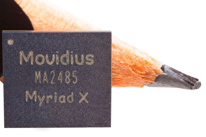
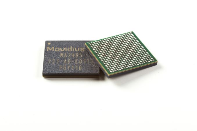
| 11:00a | Intel Announces Movidius Myriad X VPU, Featuring ‘Neural Compute Engine’
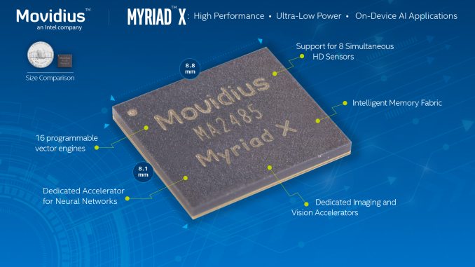
Today, Intel subsidiary Movidius is announcing the Movidius Myriad X vision processing unit (VPU), a low-power system-on-chip (SoC) intended for deep learning and AI acceleration in vision-based devices such as drones, smart cameras, and VR/AR headsets. This follows up on last month’s launch of the Myriad 2 powered Movidius Neural Compute Stick. As for the Myriad 2, the Myriad X will coexist alongside its predecessor, which was first announced in 2014. Movidius states that the Myriad X will offer ten times the performance of the Myriad 2 in deep neural network (DNN) inferencing within the same power envelope, while the Myriad 2 will remain a lower performance option. Under the hood, the Myriad X SoC features what Movidius is calling a Neural Compute Engine, an on-chip DNN accelerator. With it, Movidius states that the Myriad X can achieve over one trillion operations per second (TOPS) of peak DNN inferencing throughput, in the backdrop of the Myriad X’s theoretical 4+ TOPS compute capability.
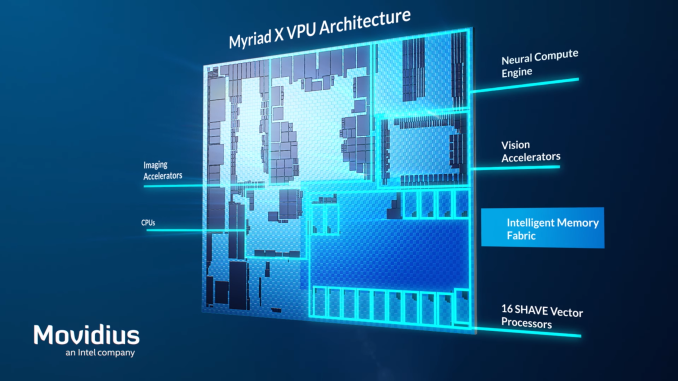
In addition, the Myriad X has four more C-programmable 128-bit VLIW vector processors and configurable MIPI lanes from the Myriad 2, as well as expanded 2.5 MB on-chip memory and more fixed-function imaging/vision accelerators. Like the ones found in the Myriad 2, the Myriad X’s vector units are proprietary SHAVE (Streaming Hybrid Architecture Vector Engine) processors optimized for computer vision workloads. The Myriad X also supports the latest LPDDR4, with the MA2085 variant equipped with only interfaces to external memory. In an accompanying launch video, Movidius locates the Myriad X functions on a stylized dieshot.
Another new function in the Myriad X is 4K hardware encoding, with 4K at 30 Hz (H.264/H.265) and 60 Hz (M/JPEG) supported. Interface-wise, the Myriad X brings USB 3.1 and PCIe 3.0 support, both new to the Myriad VPU family. All this is done within the same <2W power envelope as the Myriad 2, cited more specifically as within 1W.
At a glance, much of the Myriad X’s extra performance at the same Myriad 2 power appears to come from its new 16nm FFC TSMC process node. In shrinking from a 28nm planar process to 16nm FinFET, Movidius was able to invest the power savings into upped clocks as well as more SHAVE processors, accelerators, interfaces, and memory, all in a relatively similar package size. While Intel indeed has its own fabs, Movidius stated that the Myriad X was in development well before Intel acquired Movidius in 2016, and thus 16nm FFC was the node of choice. This 16nm FFC iteration comes after the Myriad 2’s incarnations on 28nm HPM and HPC.
While specifics were not disclosed, the Myriad X VPU comes with an SDK that includes a neural network compiler and “a specialized FLIC framework with a plug-in approach to developing application pipelines.” In any case, like the Myriad 2, the Myriad X will be programmable via the Myriad Development Kit (MDK). At this time, there were no details about the reference kit hardware. As mentioned earlier, the Myriad 2 will not be replaced by the Myriad X. Last January, the Myriad 2 was described as costing under $10; based on the higher cost FinFET process and additional hardware features, the Myriad X will likely command a higher price for the higher performance. Update (8/28/17): An Intel representative has given an update stating that 8.1mm x 8.8mm are the correct dimensions for the Myriad X VPUs. The original specifications (8.5mm x 8.7mm) that were given out were incorrect. The press kit photo has been updated. | |||||||||||||||||||||||||||||||||||||||||||||||||||||||||||||||||||||||||||||||||||||||||||||||||||||||||||||||||||||||||||


| << Previous Day |
2017/08/28 [Calendar] |
Next Day >> |