[Most Recent Entries] [Calendar View]
Monday, May 21st, 2018
| Time | Event | ||||||||||||||||||||||||||||||||||||||||||||||||||||||||||||||||||||||||||||||||||||||||||||||||||||||||
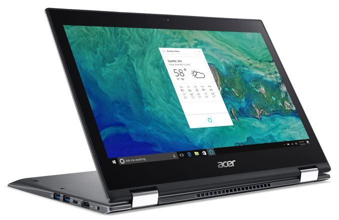
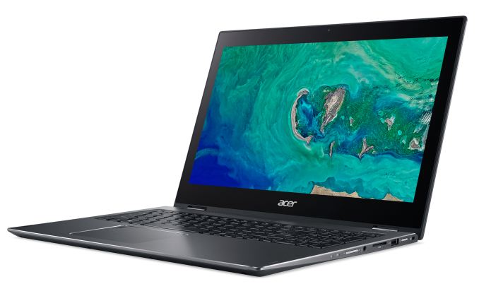
| 9:00a | Acer To Roll Out Amazon Alexa To All PCs
This morning Acer announced that it’s the first PC maker to ship Alexa on its PC lineup, and the company has plans to bring the popular assistant across its lineup of devices. Amazon has broadened the reach of Alexa across many device types over the last couple of years, and while Microsoft has shipped Cortana in Windows 10 since launch, it’s failed to gain much traction outside of the PC.
Acer will leverage Intel’s Smart Sound Technology with an integrated Digital Signal Processor to handle audio, and voice commands. Some models, such as the Acer Spin 5 will offer four digital microphones as well for far-field voice recognition, while others will only support the more common two microphone setup for near-field.
It remains to be seen whether voice control on the PC is going to be a make or break feature, but the simplicity of voice control for some tasks is undeniable. With the inclusion of Intel Smart Sound Technology, it also brings additional features such as being able to wake a PC that’s in Modern Standby as well, and with the far-field microphone, accessing Alexa on the PC should be the same as using it in your living room or kitchen. Alexa will be available on the Acer Spin 5 on May 23, and the Spin 3 on May 26, with other models gaining support over the next few weeks. Source: Acer | ||||||||||||||||||||||||||||||||||||||||||||||||||||||||||||||||||||||||||||||||||||||||||||||||||||||||
| 11:00a | The ASUS Z370-I Gaming Review: Mini-Me Mega Motherboard The ASUS ROG Strix Z370-I Gaming is one of the major Mini-ITX options for Intel's latest Coffee Lake processors. ASUS has a good history of building substantial Mini-ITX offerings, particularly with the ROG Impact line, however it is the Z-series mainstream Mini-ITX models that are the more cost effective option. For this generation, ASUS is combining dual M.2 slots, USB 3.1, EMI shielded audio and Wi-Fi on this small square platform. In this review we put it through its paces.
| ||||||||||||||||||||||||||||||||||||||||||||||||||||||||||||||||||||||||||||||||||||||||||||||||||||||||
| 4:30p | Intel And Micron Launch First QLC NAND: Micron 5210 ION Enterprise SATA SSD
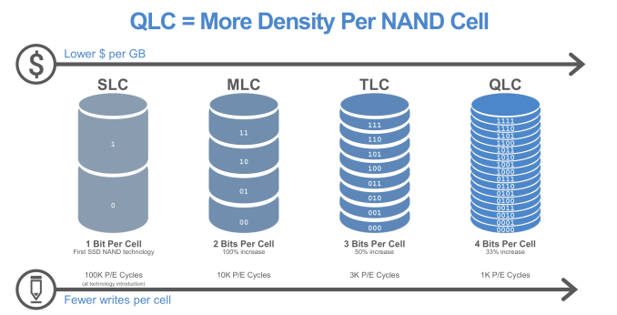
Intel and Micron are announcing today that their jointly-developed QLC NAND flash memory is now available, and Micron is now shipping the first solid state drive based on QLC NAND: an enterprise SATA drive branded the 5210 ION series. This will join the TLC-based 5200 family as a lower-cost tier with reduced write performance and endurance. QLC NAND flash memory stores four bits of data per memory cell, providing a 33% capacity boost over three bit per cell TLC NAND, which is now used in almost all SSDs. The downsides are that QLC NAND has lower write endurance on the order of 1000 program/erase cycles, and lower write performance. Both of these are consequences of the difficulty of discriminating between 16 possible voltage levels within a memory cell, as compared to the 8 voltage levels required to store three bits per cell.
The cost reduction brought by QLC NAND is a much-awaited advance for enterprise storage. Most NAND flash manufacturers have started sampling QLC NAND within the past year, generally built on the same 64-layer 3D NAND processes that current-generation TLC NAND uses. Micron has previously shown wafers of 512Gb 64-layer QLC when announcing the addition of QLC to their roadmap, but today they are also announcing a 1Tb 64L QLC part—the first 1Tb memory chip to hit commercial availability. That 1Tb part is organized as four planes that can be processing I/O commands in parallel, compared to two planes for previous Intel/Micron NAND parts. This helps offset most of the performance loss associated with increasing per-die capacity. Thanks to the "CMOS under the array" design of Intel/Micron 3D NAND, the extra peripheral circuitry requried by doubling the number of planes doesn't add much to the overall die size. It was initially feared that QLC write endurance would be low enough that drives would need to be treated more or less as write-once, read-many (WORM) devices, requiring careful handling on the software side. With multiple manufacturers now rating their QLC NAND for around 1k P/E cycles, it is clear that QLC-based SSDs aren't too fragile and can handle many existing workloads without needing major software changes to reduce writes. Micron is primarily marketing the 5210 ION SSDs as replacement for hard drives, rather than replacements for any existing tier of enterprise SSD products. In this role, the 5210 ION will have clear advantages in density (with 2-8TB per 2.5" drive) and performance. QLC NAND only provides incremental improvements to cost, so the 5210 ION won't be matching 7200RPM hard drives for price per GB, but 10k RPM drives will probably be feeling the pressure, especially from TCO calculations that take into account the power efficiency advantages of SSDs. Micron isn't providing detailed specifications for the 5210 ION series at this time, but we can read between the lines. The 5210 ION series is based on the same controller and firmware platform used for the 5200 and 5100 families. That means a Marvell 88SS1074 controller, and Micron-written firmware with features like their FlexCapacity configurable overprovisioning to trade capacity for performance and endurance.
Specific performance numbers haven't been disclosed, but Micron has indicated that both random and sequential read performance will be comparable to the 5200 family—meaning the 5210 can saturate the SATA link at higher queue depths. Write performance will be lower than the 5200 ECO but still higher than what a hard drive can deliver, especially for random writes. The most important question is what the write endurance of the new QLC-based SSDs will be. The 5210 ION's endurance rating will be less than that of the 5200 ECO, which is rated for around 1 DWPD in most capacities. Micron indicates that their QLC NAND is good for around 1k Program/Erase cycles, which suggests a limit of at most about 0.5 DWPD before write amplification is taken into account. This is still higher than many consumer SSDs, where 0.3 DWPD is a typical rating for entry-level SATA SSDs with 3D TLC NAND. When used for tasks where the performance of hard drives is currently adequate, the write endurance of the 5210 ION shouldn't be much of a problem. An endurance rating of about 0.1 DWPD would be sufficient for the 5210 ION to handle more random writes over its 5-year warranty than a hard drive can provide, but for sequential workloads it will still be possible to wear out the 5210 by writing to it at hard drive speeds. But Micron isn't recommending the 5210 ION for continuous video recording; instead they are pitching it for workloads that are at least 90% reads. The Micron 5210 ION is now shipping to select customers with capacities from 1.92TB to 7.68TB, and will be broadly available this fall. Exact pricing and specifications will be released at that time. Intel has not yet announced any products using QLC NAND, but we expect product announcements and possibly shipments in time for Flash Memory Summit in August. Intel and Micron are also working on their next generation 3D NAND manufacturing process, which increases the layer count to 96. This will provide a bigger density boost than a switch from TLC to QLC. It appears that development is currently focused on 96L TLC parts of unspecified capacity, but they will surely be followed by 96L QLC parts as well. Beyond 96 layers, Intel and Micron's long-standing partnership in flash memory technology will come to an end, with the two companies developing their flash independently. Neither company has shared any roadmap information going past this split, so it is not clear to what extent their designs will diverge with what will probably be the 128-layer generation. | ||||||||||||||||||||||||||||||||||||||||||||||||||||||||||||||||||||||||||||||||||||||||||||||||||||||||
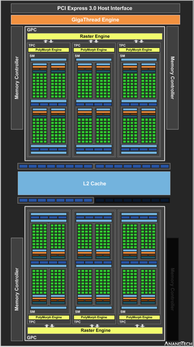
| 5:15p | NVIDIA Releases the GeForce GTX 1050 3GB: More RAM, Fewer ROPs?
Adjusting their GeForce GTX 1050 Family info page over the weekend, NVIDIA quietly announced that the expansion of the GeForce 10-series of cards with another entry: the GeForce GTX 1050 3GB. Slotting between the GeForce GTX 1050 Ti and original GeForce GTX 1050 (2GB), the GTX 1050 3GB is, despite the name, not actually equal to the original GTX 1050 2GB. Instead it features 768 CUDA cores but on a smaller 96-bit memory bus. If this story sounds familiar, it’s because it is. After launching the GTX 1060 in July 2016, NVIDIA followed up with the GTX 1060 3GB, which featured 1152 CUDA cores to the GTX 1060 6GB’s 1280.
Going down to the silicon, the GeForce GTX 1050 3GB does indeed feature 3GB of VRAM, an extra GB over the original GTX 1050, which in turn only ever came in a 2GB version in the desktop space. But ultimately, the GTX 1050 3GB is another GPU configuration: the card has an extra enabled SM – now matching the GTX 1050 Ti at 6 SMs/768 CUDA cores – while also equipped with a cut-down 96-bit bus as opposed to the 128-bit bus of its other desktop GTX 1050 series siblings. In actual memory bandwidth numbers, this translates to 84 GB/s as opposed to 112 GB/s. Otherwise, the raster engine and TMU counts are presumably identical to the GTX 1050 Ti, as the SM count requires the frontend to be a fully enabled GP107 part. As for clockspeeds, the GTX 1050 3GB features faster base and boost than both GTX 1050 Ti and GTX 1050 2GB. Things get a bit trickier on the backend though. While NVIDIA's published specifications don't offer clarity on this, the company's designs normally have a 1:1 ratio between ROP partitions and memory controllers. Meaning that as this configuration has a 96-bit memory bus – and thus only 3 out of 4 memory controllers are enabled – then it has almost certainly lost a ROP partition as well. This also means that a quarter of the GPU's L2 cache (256KB) has also been shut off, leaving the chip with just 768KB of L2. This is a prime example of why unusual memory configurations are more important than they may seem at first, as several parts of the GPU are strongly bound to the size of the memory bus. It also means that estimating the card's performance based on just clockspeeds and functional block counts is harder than it may seem, as now one needs to take into account memory bandwidth, ROP throughput, and cache hits.
All told, the existence of this card is not entirely unexpected, but it is odd. That NVIDIA is going with a 3 memory channel configuration stongly implies that the company has built up a stockpile of GP107 parts with one bad ROP/L2/MC partition, which is not unusual but GP107 is also a small enough die that the need to salvage to this level isn't quite as great. Otherwise, NVIDIA could have produced a 3GB card with a 128-bit memory bus and unbalanced memory configuration (2x1GB + 2x0.5GB), which brings its own tradeoffs but is generally the more straightforward option. At any rate, it's rare to see a salvage part like this enter the retail market this late in the cycle. In total, NVIDIA cited the performance difference to PCWorld as averaging out to around 10% uplift of the GTX 1050 3GB over the 2GB. And so once again, we are now looking at multiple GPU configurations being sold at retail under a GTX 10x0 banner. Contextually speaking, this new SKU comes in at a time of cryptocurrency mining demand, which has inflated prices and reduced availabilities for video cards all around. In that sense, where there may not have been room for an in-between GTX 1050 SKU, there is now. Or given diminishing cryptodemand, silicon that could be re-configured for consumer GeForce use. And in terms of competition, the GTX 1050 series match up with the AMD Radeon RX 560 (16 and 14 CU variants), a nominally single SKU which amusingly has had its own share of naming troubles. Lastly, recent NVIDIA GeForce launch cadence would suggest that the post GeForce GTX 10-series are on the horizon, a situation where Pascal-based lower-end product launches are easily compatible with. And for NVIDIA’s part, a quick look at their own Linux driver documentation of supported GPUs by PCI ID shows the amount of variants and configurations for GP107 and GP106, with some device IDs implying GP104-based GTX 1060 cards. Though not all of the PCI IDs may reflect a currently-selling product, some might be regional or simply unpublicized; for the rumored GTX 1060 5GB, it had already found itself on NVIDIA’s driver support lists earlier this year. So the appearance of another configuration isn’t necessarily out of the blue. For the GTX 1050 3GB today, it may not be based on GP107, and given that most manufacturers rarely, if ever, comment on the lowest performing parts in their stack, future clarification is unlikely. But while strange GPU configurations at the lower-half of performance brackets are not uncommon, as is the dearth of clear specification documentation, the obfuscating nomenclature is less palatable. As mentioned at the time of the GTX 1060 3GB launch, NVIDIA hadn’t had multiple GPU configurations selling under a single retail GTX model number for some years now, but now they’ve done it again – excluding the recent naming shenanigans with entry-level GT 1030 GDDR5/DDR4 as well as the MX150 variants. Keeping the different GPU configurations separate to the memory configuration like with the GTX 1060 is still unintuitive or misleading for most consumers, who may not research entry-level components or be unaware of how GPUs are configured. It appears that NVIDIA has no intention of changing from its ongoing nomenclature philosophy. Going forward, however, this approach hardly educates the consumer. For one, all previous references to the “GTX 1050” would need to be updated; on the GTX 1050 Family page, the performance graphs still refer to the “GTX 1050,” something that undiscerning readers would not pick up on. As noted to PCWorld in response to availability and pricing, the GeForce GTX 1050 3GB will be in the same price bracket as the GTX 1050 Ti and GTX 1050 2GB. | ||||||||||||||||||||||||||||||||||||||||||||||||||||||||||||||||||||||||||||||||||||||||||||||||||||||||
| 9:15p | ASUS Retires Radeon “AREZ” Brand: ROG Reigns Supreme
Not long since the termination of NVIDIA’s ill-fated GeForce Partner Program (GPP), over the weekend ASUS quietly announced via Twitter that the “AREZ” brand is to be retired, indicating that products would fall back under the “Republic of Gamers” umbrella. After NVIDIA announced the GPP in March, AIB partners had begun to rebrand their AMD Radeon cards and seemingly separate them from their established gaming sub-brands, pursuing the general GPP goal of aligning GeForce products to GeForce-exclusive brands. The highest profile example happened to be ASUS, where this corresponded to new AREZ and the established ROG brands – leading AMD to announce its “Freedom of Choice” advertising initiative.
As it originally panned out, ROG STRIX was replaced by AREZ STRIX, and elsewhere it was noted that Gigabyte had dropped “Aorus” and MSI had dropped “Gaming” from Radeon products. To that end, when NVIDIA finally terminated the program at the beginning of the month, the pending dissolution of AREZ was a logical conclusion, though by no means a certain one. By nature, the business dealings between GPU manufacturers and AIB partners/OEMs are largely private, where GPP’s public demise may have little to do with the underlying agreements. And therein lies NVIDIA’s credibility issue with GPP, a program that had the ostensible public goal of consumer transparency. Whatever the written or unwritten GPP stipulations were, NVIDIA did not seem interested in divulging the details necessary to correct the rampant speculation – and maintaining public silence only added to the secrecy. Likewise, OEMs and board partners had little to gain by independently commenting on the matter.
AMD, for that matter, has been limited in its public actions as they would not want to directly or indirectly damage their own relationships with the same OEMs and AIB partners, especially if it resulted in forcing them to ‘pick sides.’ Hence, with the “Freedom of Choice” re-framing of Radeon containment brands with a positive spin, as opposed to pressuring AIB partners to defy NVIDIA by keeping Radeon under the original branding. In that way, positioning AREZ in that manner let AMD respond while ASUS stayed in NVIDIA’s good graces, as officially NVIDIA did note that they did not care as long as it was a GeForce-only brand. Inasmuch as social media is a sometimes-official-sometimes-not mouthpiece, in a later reply the ASUS AREZ Twitter account did call out GPP by name, providing perhaps the closest that we will get to any official confirmation about the nature of exclusive GPP branding. But at least for consumers, the ROG ecosystem and community is once again neutral to GeForce or Radeon. The fate of other sub-brands remains to be seen.
| ||||||||||||||||||||||||||||||||||||||||||||||||||||||||||||||||||||||||||||||||||||||||||||||||||||||||


| << Previous Day |
2018/05/21 [Calendar] |
Next Day >> |