[Most Recent Entries] [Calendar View]
Monday, August 6th, 2018
- MSI Z370 Motherboards Now Support Intel’s 9th Gen Core CPUs
- Analyzing Z370 for Intel's 8th Generation Coffee Lake: A Quick Look at 50+ Motherboards
- Intel 8th Generation and 9th Generation Processor Lists Leaked: Coffee Lake Refresh?
- Intel Outs Z390 & X399 PCHs for Cannon Lake & Coffee Lake CPUs
- Intel Documents Point to AVX-512 Support for Cannon Lake Consumer CPUs
- Intel Officially Reveals Post-8th Generation Core Architecture Code Name: Ice Lake, Built on 10nm+
- ASUS Publishes List of Upcoming Intel Z390-Based Motherboards
- Samsung Discloses First Details About QLC-Based Client & Server SSDs
- Intel Details Upcoming SSDs For Datacenter Including QLC NAND
- Samsung Begins Mass Production Of 96L 3D NAND
- Western Digital Begins to Sample QLC BiCS4: 1.33 Tbit 96-Layer 3D NAND
- Intel Teases Upcoming QLC SSD For Datacenters
- We Found a Prototype 4 TB Intel QLC SSD
- Intel QLC NAND Updates: Up to 20TB In 2.5-inch SSD
- Intel And Micron Launch First QLC NAND: Micron 5210 ION Enterprise SATA SSD
- Toshiba's 768Gb 3D QLC NAND Flash Memory: Matching TLC at 1000 P/E Cycles?
| Time | Event | ||||||||||||||||||
| 7:00a | Motorola Enables 5G: A Moto Mod for the z3
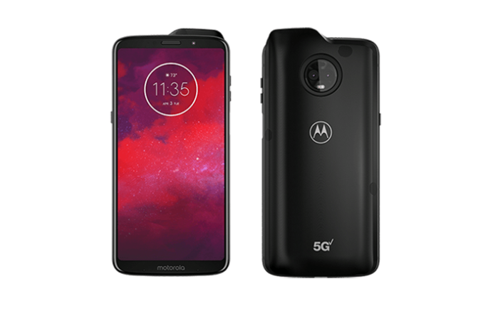
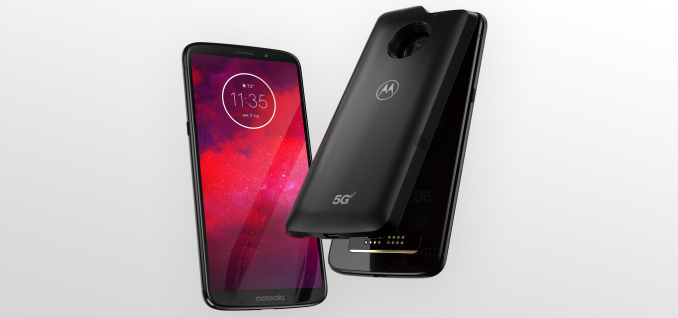
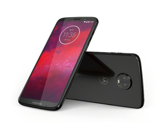
The concept of modular phones has gone from non-existent, to completely modular everything, and back again. The more you can embed into a phone at once, the slimmer the design and often everything ends up being efficient. Where modularity makes sense is when the ecosystem is large enough, and the optional mods to choose from actually make some sense. Motorola has been running its Moto Mod collection for at least two years now. The modular component is on the rear of the phone, which limits the smartphone dimensions if mods are designed to be transferred from one generation to another, but in the Moto Mod arsenal includes a bigger battery, a Hasselblad camera, big speakers, and now is set to include a 5G modem and antenna array. One of the main differences between current modem and antenna technology and 5G is the size – implementing 5G will require a good amount of power and space, and as a result most analysts have to this point expected 5G to come to industrial and large use cases first. However Motorola has announced that one of the future mods, coming in 2019, will be a US 5G capable add on for the moto z3. Inside the unit will be Qualcomm’s Snapdragon X50 mmWave 5G-capable modem and QTM052 mmWave antenna solution, along with 2000 mAh of extra battery.
The new mod, according to Motorola’s press release, will promise uninterrupted 4K live streaming, lag-free gaming, VR experiences, and the fastest download speeds ever, using the Verizon 5G network. Motorola has yet to announce pricing or specifications beyond the design, such as weight and effect on battery life, but states it will be ‘ready’ in early 2019. The state of Verizon’s 5G network will also be a question mark, and likely limited to particular regions of cities to begin with. The Moto Z3 (Stylized as moto z3)For the smartphone to attach the 5G modem to, Motorola’s new moto z3 is a 6-inch 2280x1080 smartphone running an 18:9 aspect ratio and an OLED display. Inside is a Snapdragon 835 with 4GB of LPDDR4X memory and 64 GB of UFS 2.1 storage. The front glass is Gorilla Glass 3, with an 8MP f/2.0 wide-angle (84-degree) camera on the front. The rear cameras consist of a 12MP f/2.0 primary RGB camera and a second 12MP mono-chrome unit to assist with image enhancements, depth sensing, and contrast-related focus.
The smartphone will be available on Verizon for $480 retail from August 16th, with up to $300 off a new 2-year contract with a trade-in. Related Reading | ||||||||||||||||||
| 9:00a | The AMD Threadripper 2 Teaser: Pre-Orders Start Today, Up to 32 Cores The biggest news to come out of Computex, AMD’s second generation of its Ryzen Threadripper platform, is almost here. Today’s announcement is all amount images, speeds and feeds: specifications and an ‘unboxing’ announcement, leading to pre-orders a week before retail. As much as it pains me that there is an unboxing embargo before pre-orders start, here we are. Today we get to go through the on-box specifications, discuss the design, and show what AMD included in our press kit. | ||||||||||||||||||
| 10:00a | Yangtze Memory Unveils Xtacking Architecture for 3D NAND: Up to 3 Gbps I/O
Yangtze Memory Technologies Co. (YMTC) on Monday unveiled key details regarding its Xtacking architecture that will be used for its upcoming 3D NAND flash memory chips. The company's technology involves building NAND chips using two wafers: one wafer containing actual flash memory cells, which are based on a charge trap architecture, and another wafer featuring CMOS logic. Traditionally, makers of NAND flash memory produce memory array as well as NAND logic (address decoding, page buffers, etc.) on one wafer using a single process technology. By contrast, YMTC intends to make their NAND array and NAND logic on two different wafers using different process technologies, and then bond the two wafers together, connecting the memory arrays to the logic by metal vias using one additional process step. The Xtacking architecture is designed to allow YMTC to get ultra-fast I/O while maximizing the density of their memory arrays. The manufacturer says that its 64-layer 3D NAND chips feature I/O speed of 3 Gbps, which is over two times faster when compared to Samsung’s latest V-NAND chips and about three times faster than mainstream 3D NAND. In addition, by locating the controlling logic beneath the NAND memory array, YMTC says that the Xtacking architecture allows them to maximize ttheir 3D NAND capacity and minimize dimensions of its chips. On paper, the high I/O performance would allow SSD vendors to make low-capacity SSDs with limited NAND channels without today's performance penalty, offsetting the low parallelism with high transfer rates. YMTC says that usage of two 300-mm wafers instead of one does not increase production costs significantly, as maximizing their memory density allows them to offset the cost of an additional logic wafer. Behind the scenes, the company uses XMC's fabs to produce both memory and logic. YMTC says that it uses a 180-nm process technology developed by XMC to produce the periphery logic.. Meanwhile, like other makers, YMTC does not disclose lithography node it uses for 3D NAND, but typically these manufacturing technologies are pretty ‘rough’ (~ 50 nm) by today’s standards. Because both wafers are processed using mature fabrication technologies, YMTC does not need a very high mix-and-match overlay precision to bond them together and form interconnect vias. Makers of memory in general tend to keep their die sizes low in a bid to be more competitive and profitable. When it comes to the usual Gb-per-mm2 metrics in case of planar NAND, a smaller die wins in terms of costs because the costs of the wafer are spread out over more chips (of course, putting all complexities and yield rates aside). It gets trickier with 3D NAND as wafers spend more time in chemical vapor deposition (CVD) machines, hence the number of wafers processed by a fab as well as the costs of wafers themselves are no longer crucially important metrics. Nonetheless, they are important enough for companies like YMTC to maximize its NAND density by placing the controlling logic under the memory array. Related Reading: | ||||||||||||||||||
| 11:48a | MRAM Developer Day, Everspin Keynote: The MRAM Revolution (9:15am PT, 4:15pm UTC) Prior to Flash Memory Summit, the first order of business is the MRAM Developer Day. The key talks today revolve around Everspin, a leader in MRAM Technology, GlobalFoundries, and IBM. First up is Kevin Conley, CTO of Everspin, covering the latest in the 'MRAM Revolution'. The presentation starts at 9:15am PT, and Billy and I are here to cover the event. Stay tuned for our Live Blog! | ||||||||||||||||||
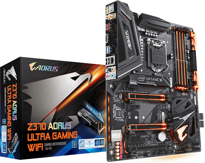
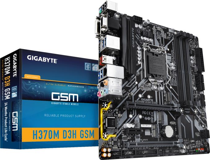
| 12:00p | GIGABYTE Adds Support for Intel’s 9th Gen Core Processors to Existing Motherboards
GIGABYTE has released new BIOS versions for its motherboards based on Intel’s 300-series chipsets, which add support for the upcoming 9th Generation Core i3/i5/i7 processors. The release reaffirms that Intel’s forthcoming CPUs will work on motherboards that are already available. As of now, 58 motherboards from GIGABYTE based on Intel’s Z370, H370, B360, and H310 chipsets support Intel’s upcoming Core i3/i5/i7 9000-series processors with the latest BIOS (see the whole list in the table below). Previously MSI added support for Intel’s new CPUs to its Z370-based mainboards.
Intel is expected to announce its 9th Gen Core processors in the coming weeks. The new chips will rely on Intel’s Coffee Lake/Kaby Lake microarchitecture, will feature up to eight cores, and will be made using a 14 nm process technology. Intel has not formally confirmed specs or features of its upcoming chips.
Related Reading: | ||||||||||||||||||
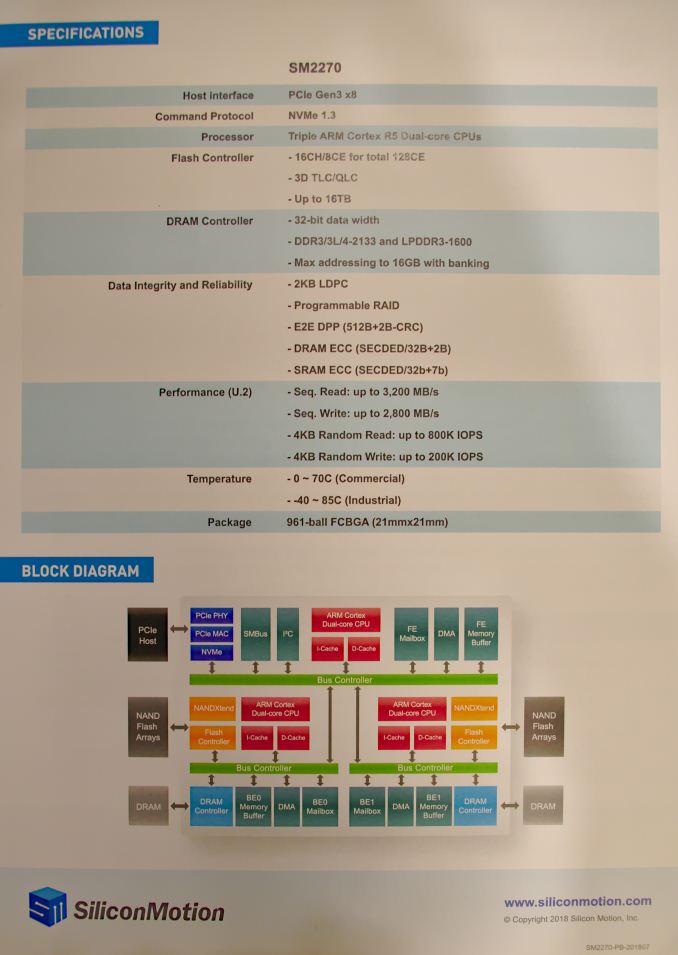
| 12:15p | Silicon Motion Announces SM2270 Enterprise NVMe SSD Controller
At Flash Memory Summit this week, Silicon Motion is previewing their first SSD controller designed specifically for enterprise and datacenter SSD. The new SM2270 will be Silicon Motion's largest and most powerful SSD controller yet, with a 16-channel NAND interface and support for a PCIe 3.0 x8 host interface. We first learned of the SM2270's existence last year when a technical presentation from Silicon Motion mentioned the next-generation LDPC error correction engine developed for the SM2270 and SM2264 controllers.
The block diagram for the SM2270 reveals an unusual structure with three separate dual-core ARM Cortex R5 CPUs. It appears that the SM2270 is organized as two 8-channel SSD controllers each with their own CPU and DRAM controller. This isn't the first dual-controller sort of architecture we've seen: Marvell is using a similar strategy with their dual-die 88SS1088 controller. In both cases, the new controllers seem designed to target Microsemi's Flashtec NVMe SSD controllers but without incurring the expense of a whole new design for a large-scale controller. | ||||||||||||||||||
| 12:37p | MRAM Developer Day, GlobalFoundries Keynote Live Blog Second Keynote today is from GlobalFoundries, Everspin's MRAM partner. | ||||||||||||||||||
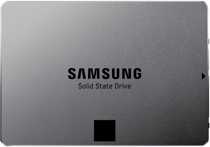
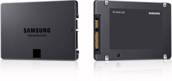
| 1:00p | Samsung Starts Mass Production of QLC V-NAND-Based SSDs
Samsung on Monday announced the industry’s first consumer SSDs based on QLC V-NAND memory. The drives will be available with capacities of up to 4 TB and will target mainstream PCs featuring a SATA interface. The new Samsung QLC SSDs are based on the company’s 1 Tb 64-layer QLC V-NAND flash as well as a proprietary controller previously used for drives powerd by 64-layer TLC V-NAND memory—probably the MJX controller from the 860 EVO. The SSDs will be available in 1 TB, 2 TB, and 4 TB configurations featuring up to 32 NAND chips. The drives come in 2.5-inch/7-mm form-factor and therefore are compatible with desktops and laptops that have a spare SATA connector. The manufacturer promises that later this year it will offer M.2 SSDs featuring its QLC V-NAND memory, but does not elaborate.
Since we are dealing with a SATA drive, its performance is not that high. Samsung’s QLC SSDs offer up to 540 MB/s sequential read speed as well as up to 520 MB/s sequential write speed when the company’s TurboWrite SLC caching technology is enabled. Random I/O speeds have not yet been disclosed. Since Samsung is only beginning to mass produce its QLC SSDs, the company does not disclose its official model name and does not disclose expected MSRPs. Keeping in mind that QLC V-NAND is supposed to provide lower costs per bit than MLC and TLC V-NAND, it is logical to expect Samsung’s QLC SSDs to be more affordable than the company’s terabyte SSDs that use MLC and TLC V-NAND memory. Related Reading: | ||||||||||||||||||
| 1:17p | MRAM Developer Day, IBM Keynote Live Blog Third Keynote in this session is from IBM Research: STT-MRAM is Ready for Applications Today. | ||||||||||||||||||
| 3:00p | Synaptics' Next-Gen Fingerprint Sensor Security: The FS7600 Match-In-Sensor
Synaptics last month introduced its second-generation match-in-sensor (MIS) solution designed for a wide range of fingerprint sensors including those in PCs and other devices. The new FS7600 MIS relies on a brand-new silicon, which the company claims is designed for maximum performance and security. | ||||||||||||||||||
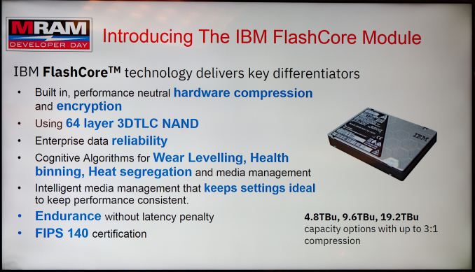
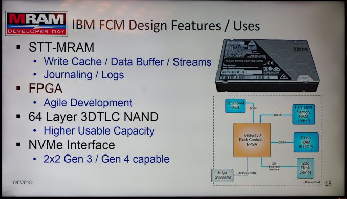
| 3:55p | IBM And Everspin Announce 19TB NVMe SSD With MRAM Write Cache
A new generation of IBM's FlashSystem storage appliances will be adopting a new architecture with magnetoresistive RAM (MRAM) write caches instead of capacitor-backed DRAM. MRAM is one of the fastest and highest-endurance nonvolatile memory technologies currently available, but it has severely limited density compared to NAND flash memory or Intel's 3D XPoint memory. Until recently, most applications of MRAM were in embedded systems where MRAM could replace small flash chips or battery-backed DRAM and SRAM buffers. Everspin, the only current supplier of discrete MRAM chips, has been pushing capacities higher with their currently available 256Mb chips and 1Gb chips that will be sampling by the end of this year. This is being enabled by their migration from in-house manufacturing on wafers fabbed at Freescale to a partnership with GlobalFoundries to make MRAM on their 22nm FD-SOI process. These capacity increases have made MRAM more attractive for use in systems that deal with a high volume of data, even though they are still far too small to be used as primary storage. IBM's existing FlashSystem appliances have used custom form factor SSDs and a system-wide power loss protection design, along with FPGA-based controllers. The new system switches to a standard 2.5" U.2 drive form factor, which requires implementing power loss protection at a per-drive level. IBM found it impractical to include enough supercaps to keep the FPGA controller running long enough to flush their DRAM write caches, but the inherent nonvolatility of MRAM eliminates the need for any bulky supercaps.
The new SSDs for IBM's FlashSystem have a usable storage capacity of up to 19.2TB of 64L 3D TLC NAND flash memory, making them some of the highest-density TLC-based drives. The drives use a 20-channel NAND interface and a four-lane PCIe 4.0 host interface that can operate in dual-port 2+2 mode. IBM's controller also provides optional transparent compression with a typical 3:1 compression ratio, and FIPS 140 compliant encryption. The new FlashSystem drives will be on display this week at Flash Memory Summit and will be shipping to customers this month. | ||||||||||||||||||
| 5:00p | More Details About the ZhongShan Subor Z+ Console, with Custom AMD Ryzen SoC
One of the exciting elements from last week’s coverage was the announcement of the upcoming Chinese market PC and Console, from Zhongshan Subor, featuring some AMD custom silicon. Through an integrated project between the two companies, being reported as a 400 million RMB investment, the custom silicon from AMD includes four Zen cores running at 3.0 GHz, along with integrated Radeon Vega graphics with 24 compute units running at 1.3 GHz, which should be good for 4 TFlops. This announcement was made at ChinaJoy, the Chinese equivalent of E3, and since the news first came to light there has been some more information coming through. | ||||||||||||||||||


| << Previous Day |
2018/08/06 [Calendar] |
Next Day >> |