[Most Recent Entries] [Calendar View]
Thursday, September 6th, 2018
- Corsair Takes Over Gaming, Video Capture, & Docking Assets from Elgato
- StarTech Launches ‘Affordable’ Thunderbolt 3 ‘Mini Docks’: USB-A, GbE, DP or HDMI
- StarTech’s New Adapter Brings eSATA Storage to Thunderbolt 3 PCs
- StarTech Launches Thunderbolt 3 USB Hub with 3 USB 3.1 Controllers & Power Delivery
- StarTech's Thunderbolt 3 to Dual 4Kp60 Display Adapters Now Available
- Promise Launches TD-300 9-in-1 Thunderbolt 3 Dock: GbE, HDMI, USB 3.0, TB3 Charging & More
- OWC Launches 13-Port Thunderbolt 3 Dock: GbE, USB-A, SD Card, mDP, FireWire & More
- StarTech Unveils Dual-Display Thunderbolt 2 Docking Station with 12 Ports
- AKiTiO Displays Thunderbolt 3 to 10GBase-T Adapter
- Samsung Foundry Roadmap: EUV-Based 7LPP for 2018, 3 nm Incoming
- Arm and Samsung Extend Artisan POP IP Collaboration to 7LPP and 5LPE Nodes
- Samsung’s 8LPP Process Technology Qualified, Ready for Production
- Samsung and TSMC Roadmaps: 8 and 6 nm Added, Looking at 22ULP and 12FFC
- TSMC Details 5 nm Process Tech: Aggressive Scaling, But Thin Power and Performance Gains
- Intel Delays Mass Production of 10 nm CPUs to 2019
- TSMC Kicks Off Volume Production of 7nm Chips
- TSMC Starts to Build Fab 18: 5 nm, Volume Production in Early 2020
| Time | Event | ||||||||||||||||||||||||||||||||||||||||||||||||||||||||||||
| 8:15a | The Toshiba XG6 1TB SSD Review: Our First 96-Layer 3D NAND SSD For the second year in a row, Toshiba is the first to ship a new generation of 3D NAND. The new XG6 NVMe SSD for OEMs otherwise changes little from last year's XG5, which makes it another good all-around drive with excellent power efficiency. | ||||||||||||||||||||||||||||||||||||||||||||||||||||||||||||
| 9:00a | AMD Announces New $55 Low-Power Processor: Athlon 200GE
Everyone lines discussing headlines: the latest mainstream processor, or super 32-core behemoth, are topics ripe for deep discussion. Despite this, a lot more volume occurs in the mid-range and low-end of the product stack. Never mind $299 for a CPU, there is a lot of action that occurs under $100. With that in mind, AMD is announcing its new $55 processor with integrated graphics, designed to sit under the Ryzen 5 2200G that we tested earlier this year. The Athlon 200GE by comparison has two cores with simultaneous multi-threading, three compute units for graphics, and a 35W TDP, all for $55. | ||||||||||||||||||||||||||||||||||||||||||||||||||||||||||||
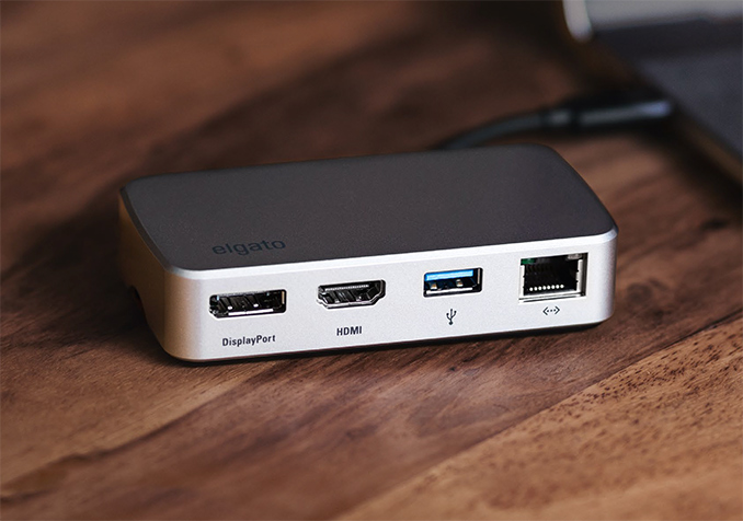
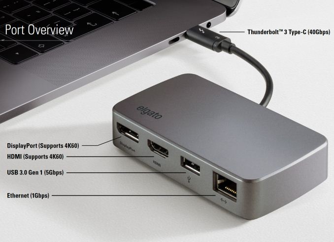
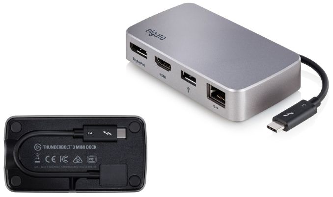
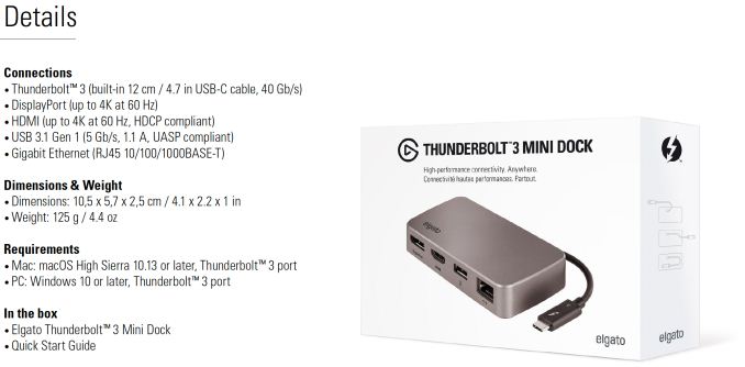
| 10:00a | Corsair Launches Elgato Thunderbolt 3 Mini Dock
Corsair on Thursday introduced its first Elgato-branded miniature Thunderbolt 3 dock. The product has two 4Kp60-capable display outputs, a USB Type-A port, and a Gigabit Ethernet connector. The minimalistic Elgato Thunderbolt 3 Mini Dock is aimed primarily at owners of Apple’s latest MacBook Pro laptops who need an essential set of ports while on the go. The Thunderbolt 3 Mini Dock has one DisplayPort 1.2 output, an HDMI 2.0 output (with HDCP support), a USB 3.1 Gen 1 Type-A port (5 Gbps, up to 1.1 A), and a GbE port.
Being very compact, the Thunderbolt 3 Mini Dock weighs 125 grams (4.4 ounces), looks like a big pack of mints, and comes with a foldable 12 cm (4.7 inch) cable that can be quickly hidden when not in use as well as easily managed when in use. When it comes to compatibility, the Elgato Thunderbolt 3 Mini Dock will work with Apple’s macOS High Sierra 10.13 or later as well as with Microsoft’s Windows 10 and later. Unfortunately Corsair does not disclose which Thunderbolt 3 controller it uses for its TB3 Mini Dock – whether they're using Alpine Ridge or the new USB 3-compatible Titan Ridge – however the exclusion of any mention of USB 3 compatibility in the official specifications strongly points to the tradtional Alpine Ridge, making this a true TB3-only dock.
Meanwhile, to make the Elgato Thundebolt 3 Mini Dock more attractive to owners of various Apple devices, the product comes with the Elgato Dock Utility for macOS that enables high-power USB support and easy ejection of storage devices attached to the dock. Corsair’s Elgato Thunderbolt 3 Mini Dock will hit the market shortly. In the U.S. it will cost $149, while in other countries prices will be different.
Related Reading: | ||||||||||||||||||||||||||||||||||||||||||||||||||||||||||||
| 11:00a | Samsung Foundry Updates: 8LPU Added, EUVL on Track for HVM in 2019
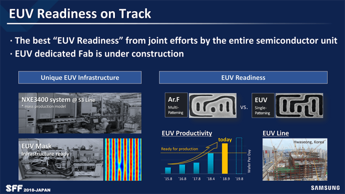
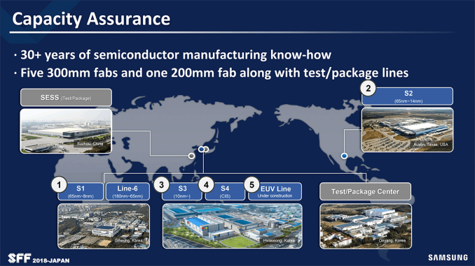
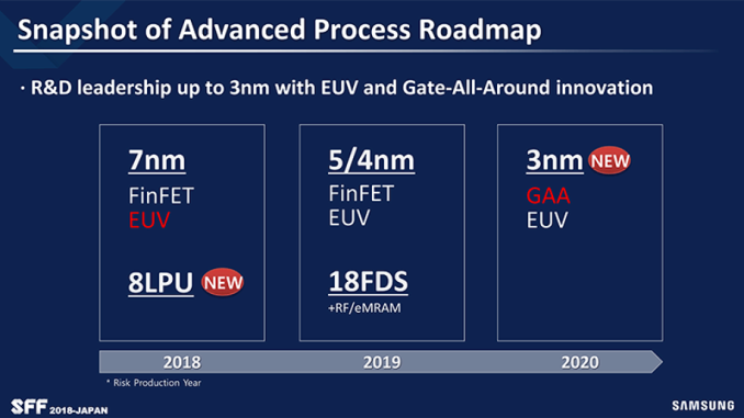
Samsung recently hosted its Samsung Foundry Forum 2018 in Japan, where it made several significant foundry announcements. Besides reiterating plans to start high-volume manufacturing (HVM) using extreme ultraviolet lithography (EUVL) tools in the coming quarters, along with reaffirming plans to use gate all around FETs (GAAFETs) with its 3 nm node, the company also added its brand-new 8LPU process technology to its roadmap. 10 nm Node Lives OnSamsung Foundry’s general roadmap was announced earlier this year, so at SFF in Japan the contract maker of semiconductors reiterated some of its plans, made certain corrections, and provided some additional details about its future plans. First up, Samsung added another fabrication technology into its family of manufacturing processes based on its 10 nm node. The new tech is called 8LPU (low power ultimate) and, according to Samsung’s usual classification, this is a process for SoCs that require both high clocks and high transistor density. Samsung’s 8LPP technology, which qualified for production last year, is a development of Samsung’s 10 nm node that uses narrower metal pitches to deliver a 10% area reduction (at the same complexity) as well as a 10% lower power consumption (at the same frequency and complexity) compared to 10LPP process. 8LPU is a further evolution of the technology platform that likely increases transistor density and frequency potential vs 8LPP. Meanwhile Samsung does not disclose how it managed to improve 8LPU vs. 8LPP and whether it involved advances of design rules, usage of a new library, or a shrink of metal pitches. Samsung’s 8LPP and 8LPU technologies are aimed at customers who need higher performance or lower power and/or higher transistor density than what Samsung’s 10LPP, 10LPC, and 10LPU processes can offer, but who cannot gain access to Samsung’s 7LPP or more advanced manufacturing technologies that use EUVL. Risk production using 8LPU was set to start in 2018, so expect high-volume manufacturing to commence next year at Samsung’s Fab S1 in Giheung, South Korea. 7LPP EUV on TrackLast year Samsung Foundry promised to start risk production of chips using its 7LPP fabrication technology in 2018. As it appears, it has initiated manufacturing of certain 7LPP SoCs, though presumably only for its parent company, as its MPW shuttle service schedule does not mention 7LPP at all. The production tech will be Samsung Foundry’s flagship process, so expect the company to use it first for its parent company’s mobile SoCs. Meanwhile, the process tech is also suitable for larger chips aimed at HPC, ML, and AI markets (think CPUs, specialized SoCs, etc.). For example, Samsung is prepping specialized IP for appropriate chips, including 100 Gbps+ SerDes and other.
At the forum, Samsung Foundry said that it had installed multiple ASML Twinscan NXE:3400B EUVL step and scan systems at its Fab S3 in Hwaseong, South Korea. The company naturally does not disclose how many of such tools have been installed, but it indicated that wafer per day (WPD) performance of the said scanners is in line with its mass production targets. As reported before, the first manufacturing processes that will take advantage of EUVL will use it for select layers only, so do not expect extensive usage of the new equipment initially. In fact, since EUV will be used for HVM for the first time in the industry, Samsung Foundry is hardly inclined to expand its usage beyond select customers and designs (think Samsung Electronics and Qualcomm, which has already selected 7LPP for its Snapdragon 5G SoC due in 2019).
A radical expansion of EUV lithography usage by Samsung Foundry will occur after it builds another production line in Hwaseong, which will be architected for the EUV equipment from the start. The line is set to cost 6 trillion Korean Won ($4.615 billion), it is expected to be completed in 2019, and start HVM in 2020. As a result, Samsung’s production involving EUVL equipment will be limited to one fab for at least several quarters down the road. Generally, this is a reason why Samsung Foundry has developed its 8LPP and 8LPU process technologies. 5/4 nm to Hit Risk Production in 2019By the time the new production line in Hwaseong becomes operational, Samsung Foundry promises to start risk production using its 5/4 nm node. As reported earlier this year, Samsung is prepping 5LPE, 4LPE, and 4LPP fabrication technologies, but eventually this list will likely expand. Based on what Samsung has disclosed about all three manufacturing processes so far, they will have certain similarities, which will simplify migration from 5LPE all the way to 4LPP, though the company does not elaborate.
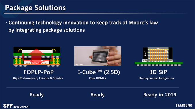
One of the slides the company demonstrated at SFF 2018 Japan indicates that Samsung expects risk production of chips using the 5/4 nm node to commence in 2019, indicating that the process technologies will coexist rather than follow each other. Since there are hardly any reason for Samsung to design competing fabrication processes, it is more likely that its 5LPE will be used for HVM first in 2020 and then 4LPE/4LPP will follow later on expanding usage of EUV equipment, unless Samsung’s roadmap changes significantly and certain offerings get canned (which tends to happen). One of the things to keep in mind is that Samsung’s 5/4 nm will be the company’s last node to use FinFET transistors, which is why it will be “long” node that will be used for many years to come, just like the 28 nm technology is used today and will stay here for a long time. 3 nm Pulled In?One of the unexpected things that Samsung Foundry announced was start of risk production using its 3 nm node already in 2020, which is at least a year ahead of what was expected earlier. Samsung’s 3 nm will be the first node to use the company’s own GAAFET implementation called MBCFET (multi-bridge-channel FETs) and will officially include at least two process technologies: 3GAAE and 3GAAP (3nm gate-all-around early/plus). Samsung still did not announce any HVM targets for 3GAAE and 3GAAP and it is hard to say when exactly the company adopts its MBCFET-based technologies for commercial SoCs. What we do understand today is that both technologies will rely on EUVL, so before using either Samsung will have to make sure that EUV delivers the necessary yields and production performance. Considering the fact that Samsung is satisfied with performance of its ASML Twinscan NXE:3400B EUVL step and scan systems today and expects further increases of WPD productivity, it is possible that it pulled in its 3 nm node. 18FDS Risk Production Due in 2019Although GAAFETs are only several years away, technologies based on planar transistors are not going anywhere and keep evolving. Samsung Foundry will continue to back FD-SOI technology going forward and will offer a formidable rival for GlobalFoundries’ 22FDX and 12FDX offerings. Samsung Foundry intends to start risk production of chips using its 18FDS already in 2019, so expect HVM in 2020 at the latest. The tech uses the same BEOL interconnects as Samsung’s 14LPE/14LPP technologies (i.e., BEOL originally developed for its 20 nm planar process), but with new transistors and FEOL. The company promises that when compared to its 28FDS, its 18FDS will enable a 20% higher performance (at the same complexity and power), a 40% lower power (at the same frequency and complexity), and a 30% lower die area. What is particularly important is that 18FDS will support both RF and eMRAM, allowing Samsung Foundry to target a wide variety of applications that require RF and embedded memory in the 5G era in 2020 and onwards. 3D System-in-Package Ready in 2019Chip packaging technologies are gaining importance these days as it becomes increasingly hard and expensive to integrate everything into a single processor. Samsung (just like TSMC and GlobalFoundries) already has a number of package solutions for complex products, such as FOPLP-PoP for mobile SoCs and I-Cube (2.5D) for chips that use HBM2 DRAMs. Next year the company will offer its 3D SiP (system-in-package) solution that will enable it to pack a variety of devices into a single three-dimensional package with a small footprint.
Samsung Foundry’s 3D SiP will be one of the industry’s first technology of its kind that will be used to build heterogeneous 3D SiPs (currently all SiPs are 2D). The package solution will enable the contract maker of semiconductors to assemble SiPs using components made using entirely different process technologies. Related Reading: Source: PC Watch | ||||||||||||||||||||||||||||||||||||||||||||||||||||||||||||
| 12:55p | UL Delists Huawei Devices Due To Inaccurate Benchmarks
A few days ago we published our article addressing Huawei and Honor’s inaccurate benchmarking behaviour. In a nutshell, we had found out that this year’s devices had introduced a new thermal limiting behaviour that quickly throttled power consumption to ~4-4.5W in 3D workloads. While this in itself wasn’t an issue, the problem is that the firmware did not apply this new behaviour to a specific list of whitelisted 3D benchmarks. Sidenote: Earlier this year, Futuremark (The 3DMark creators) had been acquired by UL, joining the global safety consulting and certification company as a benchmarking division. We work closely with all benchmark vendors, and UL isn’t an exception. We had first given UL note of the behaviour two weeks ago and had been sharing our early results with the development team. Today UL published their independent confirmation of our results on their own devices, and have subsequently decided to remove the tested devices from their results database. UL stresses that the kind of detection and optimization performed by Huawei infringes the company’s rules for manufacturers. Unfortunately this isn’t the first instance of a vendor being delisted, as most famously a slew of phone manufacturer had been delisted in 2013 after a more in-depth investigation of ours resulted in quite embarrassing results for a lot of vendors. The UL team further explains that they’ve also been in touch with Huawei, and that the Chinese vendor is planning to address the behaviour by introducing a new “performance mode” that disables the new thermal throttling behaviour. In essence this mode would revert back to the behaviour we’ve seen in the past such as the Mate 9 – where the SoC is allowed higher peak performance figures at a cost of high power. While this is still problematic for representative benchmarking for devices with Kirin 960’s and 970’s (due to the very large peak power at the highest performance states of those SoCs), I expect this to be a non-issue for the new Kirin 980, as it’s projected to have significantly better sustainable peak power figures. We're still looking forward to the new SoC in the upcoming Mate 20, and believe it to be an outstanding performer. | ||||||||||||||||||||||||||||||||||||||||||||||||||||||||||||
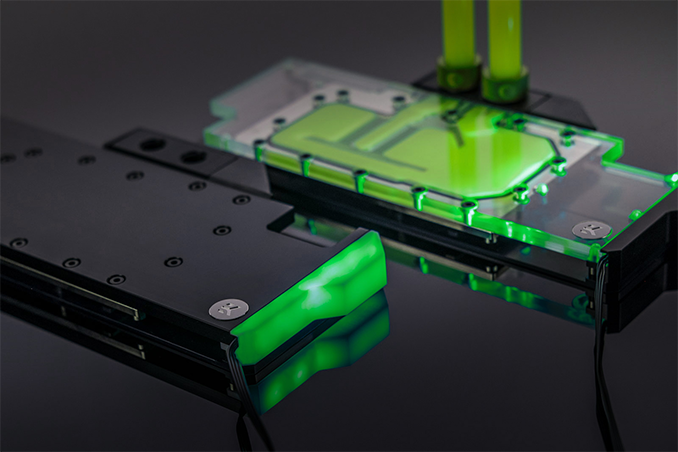
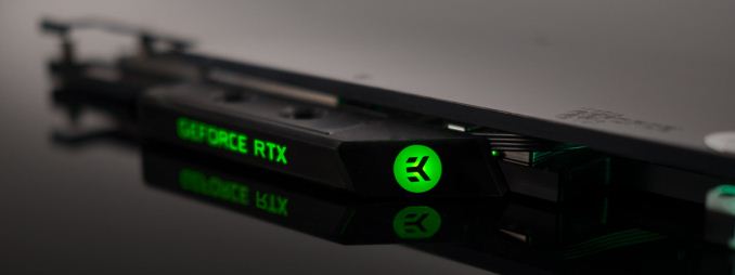
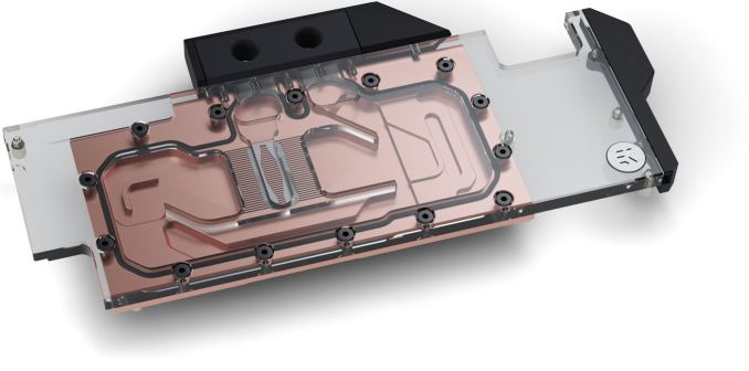
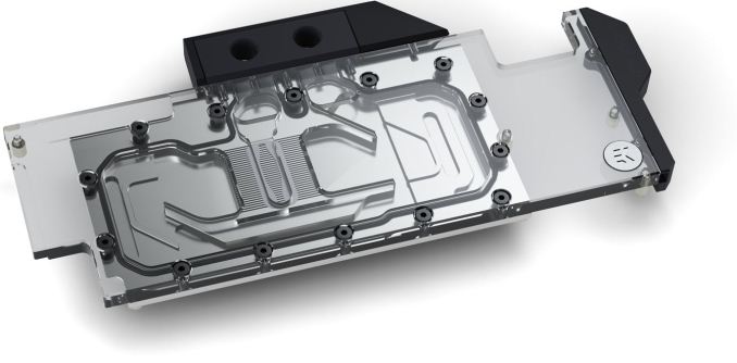
| 1:00p | EKWB Announces EK-Vector RTX Water Blocks for GeForce RTX 2080 & RTX 2080 Ti
EK Water Blocks this week announced that it will be releasing water blocks for NVIDIA’s reference design GeForce RTX 2080 and GeForce RTX 2080 Ti video cards. The EKWB EK-Vector RTX water blocks are designed for custom-built liquid cooling systems for NVIDIA’s latest graphics adapters and will hit the market later this month, offering not only improved performance for the new NVIDIA cards, but also a new look.
EKWB’s EK-Vector RTX 2080 and EK-Vector RTX 2080 Ti full-cover single-slot water blocks for NVIDIA’s reference design GeForce RTX 2080 and GeForce RTX 2080 Ti add-in-boards come in eight versions, all featuring the company’s cold plate with proprietary Open Split-Flow micro-channels. Traditionally for EKWB, the EK-Vector RTX water blocks use standard G ¼ inch barbs for tubing and are therefore compatible with a wide range of LCS setups. To further improve cooling performance, EKWB will also offer specially designed backplates.
Depending on the version, the cold plate is made of bare electrolytic copper or nickel-plated electrolytic copper, whereas the cover is made of transparent plexiglass or black acetal. Meanwhile, all versions featuring nickel-plated cold plates are also outfitted with RGB strips, which use a 4-pin 12 V connector and can be controlled by RGB command software from the leading motherboard brands (ASUS, ASRock, GIGABYTE, MSI).
As is typically the case, custom liquid cooling does not come cheap. EKWB’s EK-Vector RTX GPU water blocks will retail for €129.9 – €149.9 depending on the specific SKU, whereas the backplates will cost €39.9 – €43.9. EKWB will start shipments of its water blocks on September 20, whereas backplates will hit the market in October.
Related Reading: | ||||||||||||||||||||||||||||||||||||||||||||||||||||||||||||


| << Previous Day |
2018/09/06 [Calendar] |
Next Day >> |