[Most Recent Entries] [Calendar View]
Thursday, August 1st, 2019
- CES 2019: Thermaltake Unveils Its WaterRAM RGB Liquid Cooled DDR4-3200 Memory
- Corsair's Hydro X: Making Custom Loop Water Cooling More Mainstream
- Thermaltake Goes Big: Water 3.0 Ultimate CLC Launched, 3x120mm
- Samsung Unveils Galaxy Tab S5e: 10.5-Inch sAMOLED with USB-C
- Samsung Introduces Galaxy Tab S4: S835, 7300mAh Battery, Samsung DeX
- New Apple iPad with Pencil Support: From $299 for Students
- Apple Announces iOS 13: Dark Mode, iPadOS & Files
- The Apple WWDC 2019 Keynote Live Blog (Starts at 10am PT/17:00 UTC)
- LG Introduces New UltraFine 4K and 5K Monitors
- Logitech Unveils Slim Folio Pro Keyboard for 3rd Gen iPad Pro
- The 2018 Apple iPad Pro (11-Inch) Review: Doubling Down On Performance
- Apple Announces New 11" and 12.9" iPad Pros with A12X SoC
- G.Skill Launches Trident Neo Memory Modules for AMD Ryzen 3000 CPUs
- Patriot Unveils Viper 4 Blackout: Compatible with Ryzen 3000, Up to DDR4-4000
- The AMD 3rd Gen Ryzen Deep Dive Review: 3700X and 3900X Raising The Bar
- Toshiba & WD NAND Production Hit By Power Outage: 6 Exabytes Lost
- Toshiba Memory and Western Digital Open Fab 6 and New Memory R&D Center
- Toshiba Memory & Western Digital Finalize Fab K1 Investment Agreement
- Toshiba Begins to Construct New BiCS 3D NAND Fab in Iwate Prefecture
- Toshiba Memory to Build New Fab to Produce BiCS 3D NAND
- Toshiba Finalizes Plans for New 3D NAND Fab: Coming Online in 2019
- Toshiba to Build New Fab to Produce BiCS NAND Flash
| Time | Event | |||||||||||||||||||||||||||||||||||||||||||||||||||||||||||||||||||||||||||||||||||||||||||||||||||||||||||||||||||||||||||||||||||
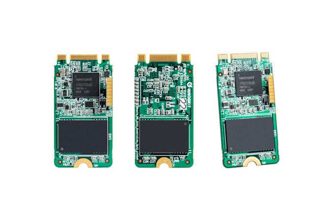
| 8:30a | Innogrit Debuts With Four NVMe SSD Controllers
A new SSD controller designer is coming out of stealth mode today. Innogrit was founded in 2016 by storage industry veterans with the goal of developing storage technology to support AI and big data applications. We spoke with co-founder Dr. Zining Wu (formerly Marvell's CTO) about the company's planned product lineup, and he will be presenting more information next week in a keynote speech at Flash Memory Summit. Innogrit's long term goal is to go after the enterprise storage market, but they are starting small with a DRAMless client SSD controller, the IG5208 "Shasta". This is already in mass production with full turnkey reference SSD designs available. It will be followed up incrementally larger controllers with more advanced feature sets: Shasta+, Rainier and Tacoma. With each iteration, Innogrit is increasing performance, adding more features and improving their LDPC error correction engine.
The Shasta and Shasta+ controllers are both primarily targeting the client SSD market, and they are designed as low-cost mainstream solutions. Shasta has just two PCIe 3 lanes while Shasta+ has four lanes and consequently higher performance, but otherwise they are quite similar. Both are 28nm designs and use the NVMe Host Memory Buffer feature rather than including DRAM controllers. Both controllers are small enough to be packaged inside single-chip BGA SSDs, and Innogrit's reference designs for Shasta-based SSDs include the standard 11.5x13mm and 16x20mm BGA SSD footprints and a CFX card design. The improved ECC capabilities of Shasta+ will make it a better choice for QLC-based SSDs, but both controllers support the full range of SLC through QLC from multiple manufacturers. Because Shasta and Shasta+ are stepping stones toward the enterprise and datacenter markets, they include support for some features not commonly found on client SSDs, such as an Open-Channel SSD operating mode. End-to-end data path protection is included, with ECC on all the controller's SRAM buffers and on data stored in the Host Memory Buffer. Power management appropriate for client and embedded use is supported, with Shasta peaking at 0.9W and supporting idle states at 55mW and less than 1mW, while Shasta+ will peak at about 1.35W. The NVMe Boot Partition feature is also supported for embedded systems that don't include a separate boot ROM device.
Innogrit's Rainier controller is a significant generational advance over the Shasta family, moving up to the high-end client and entry-level datacenter markets. Rainier switches to one of TSMC's 16/12nm FinFET processes, which Innogrit (and most other controller designers) sees as necessary for PCIe gen4 support with reasonable power consumption. Rainier has 8 NAND channels that can run at up to 1200MT/s, fast enough for any currently-available NAND. This allows for sequential read and write speeds of up to 7GB/s and 6.1GB/s respectively, more or less saturating the PCIe 4 x4 interface. Rainier adds enterprise-oriented features like multiple namespace support and SR-IOV virtualization, but client-oriented power management is still supported, with idle states for 50mW and less than 2mW. The most powerful controller on Innogrit's roadmap is Tacoma, which builds on Rainier by doubling the NAND channel count to 16 (bringing the maximum supported capacity up to 32TB), widening the DRAM interface to 72 bits (64b with ECC), and adding more high-end enterprise features. Sequential IO performance will be roughly the same as for Rainier but random IO gets a boost from the extra parallelism. The virtualization capabilities have been enhanced relative to Rainier and the NVMe Controller Memory Buffer feature is supported, which comes in handy for NVMe over Fabrics deployments. A special low-latency mode is introduced, which Innogrit will be demonstrating with Toshiba's XL-FLASH (their answer to Samsung's Z-NAND). Perhaps the most important feature of Tacoma is the addition of in-storage compute with a deep learning accelerator; more information about this will be shared next week during Innogrit's keynote presentation at Flash Memory Summit.
| |||||||||||||||||||||||||||||||||||||||||||||||||||||||||||||||||||||||||||||||||||||||||||||||||||||||||||||||||||||||||||||||||||
| 9:00a | The Ice Lake Benchmark Preview: Inside Intel's 10nm Intel's new Ice Lake platform is the company's second attempt at producing a 10nm chip for the mass market, and follows on from the Cannon Lake platform. Using 'the same but different' 10nm process, Ice Lake holds inside a new 10th Gen Core microarchitecture called Sunny Cove, Gen11 graphics, and support for LPDDR4X-3733 as well as Thunderbolt and Wi-Fi 6. In advance of systems coming onto the market, Intel gave a small number of press a day of hands-on time with its Software Development Systems so we could get a taste of performance of Sunny Cove, Gen11, and Intel's newest 10nm product. | |||||||||||||||||||||||||||||||||||||||||||||||||||||||||||||||||||||||||||||||||||||||||||||||||||||||||||||||||||||||||||||||||||
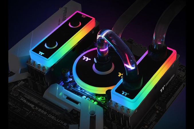
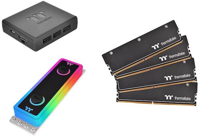
| 11:00a | Thermaltake’s Launches Liquid-Cooled WaterRam RGB DDR4-3600 Kits
Seemingly intent on proving that everything in a PC should in fact be liquid cooled, Thermaltake this week has expanded its WaterRAM lineup of water-cooled RAM with DDR4-3600 kits. Available as a 32 GB dual-channel/quad-channel kit, Thermaltake’s WaterRAM DDR4-3600 (CL-W262-CA00SW) feature CL18 19-19-36 timings and 1.35 V operating voltage. The modules are based on tightly-screened SK Hynix’s C-die memory chips, a 10-layer PCB, and feature XMP 2.0 profiles for easier overclocking.
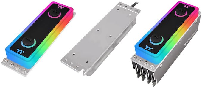
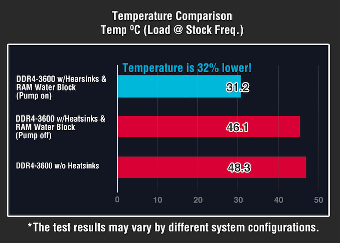
The key selling feature of Thermaltake’s WaterRAM DDR4-3600 kit is its cooling system. It includes 2-mm thick aluminum heatsinks on the modules as well as a copper nickel-plated water block with a PMMA cover that is installed on top of the DIMMs. The water block is equipped with G ¼ fittings compatible with the majority of open loop liquid cooling systems. Meanwhile, following the latest trends, the water block features 12 built-in addressable LEDs that can be controlled using Thermaltake’s hardware controller (bundled) or using software from leading motherboard makers, Razer Chroma, and Amazon Alexa.
The manufacturer says that liquid cooling allows them to reduce RAM temperatures by 32% when compared to regular heat spreaders, a claim that has to be tested independently. Ideally, lower temperatures should enable at least some higher overclocking potential and/or improve stability.
Thermaltake’s WaterRAM DDR4-3600 kit will be available shortly. The modules themselves are backed with a lifetime warranty, whereas the water block is covered with a two-year warranty. Related Reading: Source: Thermaltake (via TechPowerUp) | |||||||||||||||||||||||||||||||||||||||||||||||||||||||||||||||||||||||||||||||||||||||||||||||||||||||||||||||||||||||||||||||||||
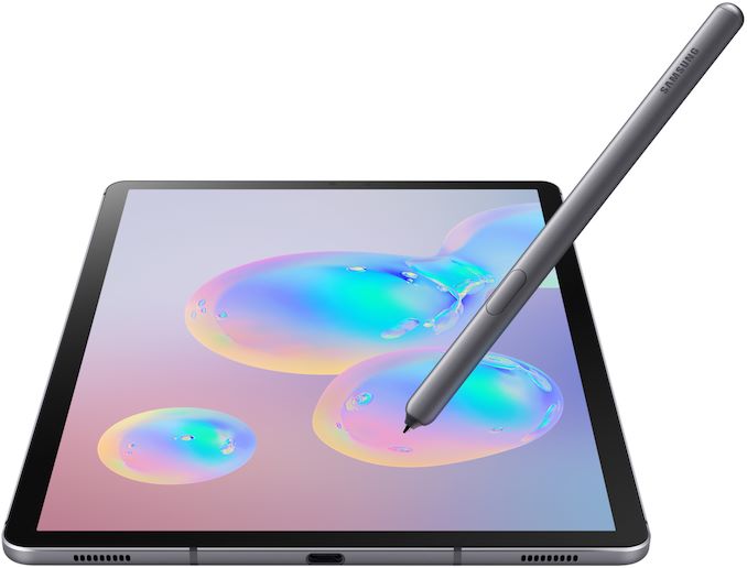
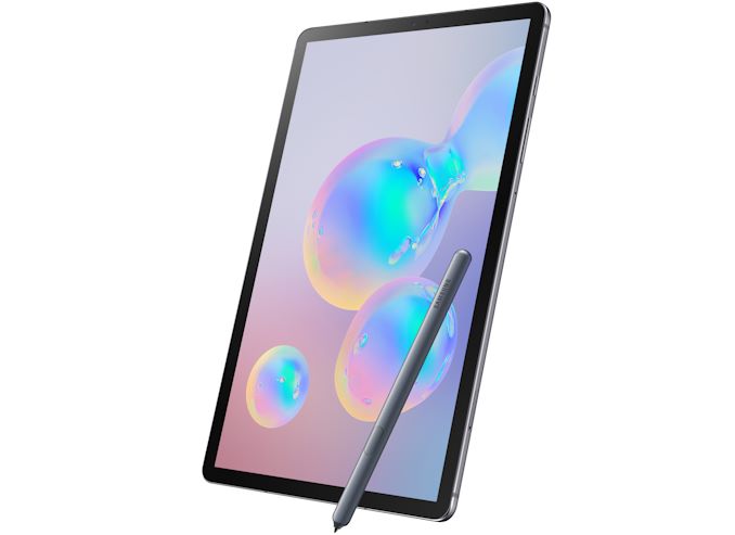
| 12:00p | Samsung Introduces Galaxy Tab S6: 10.5-Inch AMOLED, Snapdragon 855, New S-Pen
Samsung has introduced its new flagship tablet aimed at consumers that need advanced functionality and performance. The Galaxy Tab S6 comes with a large AMOLED display, Qualcomm’s high-end application processor for smartphones and tablets, plenty of storage, compatibility with Samsung’s DeX platform for productivity applications, the company’s Knox security platform, as well as Samsung’s refined S Pen stylus with remote control functionality and wireless charging. The Samsung Galaxy Tab S6 is based on Qualcomm’s Snapdragon 855 SoC featuring four high-performance cores, four low-power cores, and Adreno 640 integrated GPU. The application processor accompanied by 6 or 8 GB of LPDDR4/LPDDR4X memory as well as 128 or 256 GB of NAND flash storage (expandable using a microSDXC card). Like other high-end consumer tablets from Samsung released in the recent quarters, the Galaxy Tab S6 is equipped with a 10.5-inch Super AMOLED display with a 2560×1600 resolution, stylus support, and thin bezels. On the audio side of matters, the tablet has four speakers and two microphones.
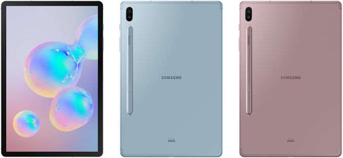
Imaging capabilities of the Galaxy Tab S6 look rather interesting. For the first time on a consumer tablet from a well-known manufacturer, the device has two camera modules on the back: a 13 MP RGB sensor and a 5 MP 123-degree ultra-wide lens. For some reason, the company decided not to equip its dual camera with a flash though. Meanwhile, there is an 8 MP camera for selfies and video calls on the front. As far as wireless connectivity features are concerned, the Galaxy Tab S6 has an 802.11ac Wi-Fi controller with MU-MIMO support, Bluetooth 5.0, as well as GPS (+ GLONASS, Beidou, Gallileo). The manufacturer claims that variants with a 4G/LTE modem will be available later this year, but does not elaborate. On the wired side of things, the tablet has a USB 3.1 Type-C interface for audio, data, and charging, as well as a set of POGO connectors for keyboards or other gear. When it comes to sensors, the Galaxy Tab S6 has an on-screen fingerprint reader, an accelerometer, a compass, a gyroscope, a proximity sensor, RGB light sensor, and so on. Since the Galaxy Tab S6 is designed primarily for consumers, it is very thin (5.7 mm), light (420 grams), and comes in consumer-friendly gray, blue, or rose enclosures.
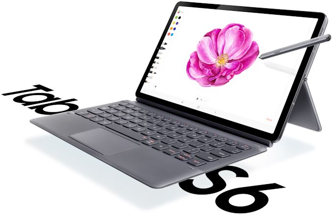
Despite it's consumer positioning, the Galaxy Tab S6 can be a very powerful tool for professionals: it comes with a new S Pen stylus that can serve as a remote controller for select applications, it support Samsung’s Knox mobile security platform to protect valuable and confidential information, and it is compatible with Samsung’s DeX platform that enables desktop-like experience on Android-based tablets (e.g., open up multiple windows, re-size windows, drag and drop content, etc.). To make usage of DeX more convenient, the Galaxy Tab S6’s dedicated book cover keyboard comes with a special DeX key to launch or close the environment. Meanwhile, there is no word whether the tablet can support an external display via its USB Type-C connector using an appropriate adapter, however since the smartphone Galaxy counter-parts support this, it's likely the Tab S6 does as well.
Samsung will start to take pre-orders on the Galaxy Tab S6 on August 23 and will start retail sales on September 6th. MSRP of the basic version of the tablet will start at $649. The new S Pen is bundled with the device, whereas the keyboard will be sold separately.
Related Reading: Source: Samsung | |||||||||||||||||||||||||||||||||||||||||||||||||||||||||||||||||||||||||||||||||||||||||||||||||||||||||||||||||||||||||||||||||||
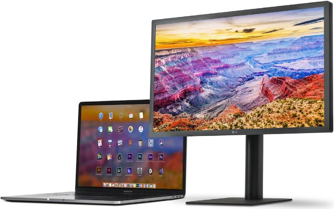
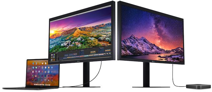
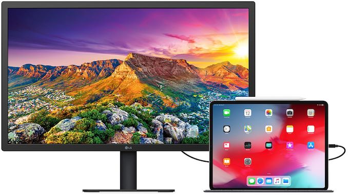
| 1:00p | LG Unveils New UltraFine 4K & 5K Monitors: Now with iPad Pro Support
LG has updated its UltraFine lineup of displays, which are aimed especially at computers made by Apple. The entry-level UltraFine 4K has received a larger screen, whereas the more advanced UltraFine 5K has gained a USB Type-C port. Both monitors are now compatible with Macs as well as the latest iPad Pro tablets, enabling owners of the latter to use them as desktops. The new entry-level LG UltraFine 4K monitor is now based on a 23.7-inch IPS panel featuring a 3840×2160 resolution, 500 nits brightness, a 60 Hz refresh rate, and the usual 178°/178° horizontal/vertical viewing angles. The display comes with integrated stereo speakers, and an built-in PSU. When compared to the original UltraFine 4K introduced in 2016, the new LCD is bigger, but its resolution is the same, and as a result the pixel density got lower.
The larger LG UltraFine 5K display uses a 27-inch IPS panel featuring a 5120×2880, 500 nits brightness, a 60 Hz refresh rate, and 178°/178° horizontal/vertical viewing angles. The new LCD is equipped with a webcam, built-in stereo speakers and a microphone, as well as an integrated power supply. In an important change, this model now no longer requires a Thunderbolt 3 connection; the monitor can be used with a USB-C port as well (with DP alt mode), making it compatible with a wider range of devices, and likely indicating that LG has upgraded to Intel's Titan Ridge TB3 controller.
As these monitors are primarily meant to be used with Apple products, LG’s UltraFine monitors only support the P3 color gamut – where Apple offers very robust OS-level support – and are compatible with Apple’s latest Macs as well as 2019 iPad Pro tablets, making this the first time these displays have worked with an iPad. Both displays can connect to hosts using a Thunberbolt 3 or a USB 3.1 Gen 1 Type-C ports that can deliver up to 85 W or 94 W of power to a laptop or a tablet.
The new LCDs are currently available from Apple. The LG UltraFine 4K 23.7-inch display is priced at $699.95, whereas the UltraFine 5K 27-inch monitor is priced at $1,299.95. Related Reading: Source: LG | |||||||||||||||||||||||||||||||||||||||||||||||||||||||||||||||||||||||||||||||||||||||||||||||||||||||||||||||||||||||||||||||||||
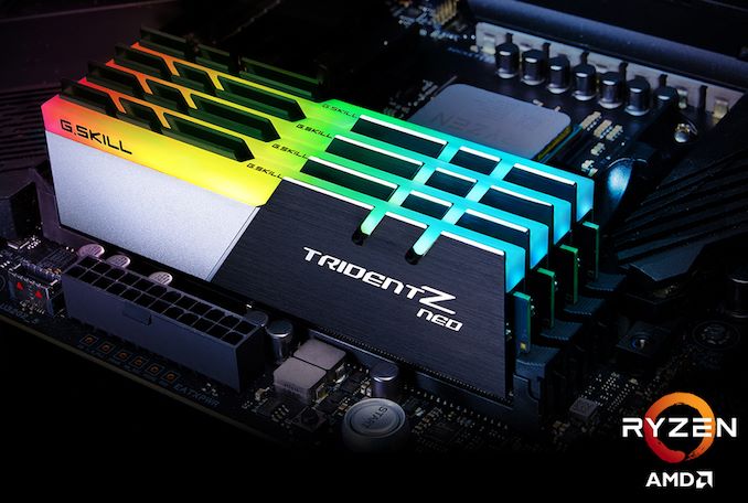
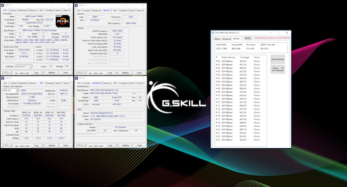
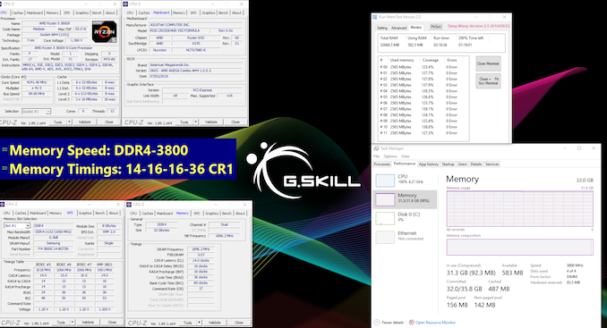
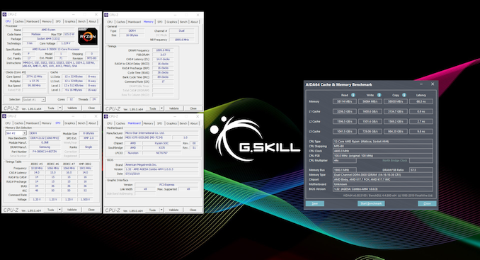
| 2:00p | G.Skill Reveals Trident Z Neo DDR4-3800 CL14 Kit for AMD Ryzen 3000
G.Skill has introduced its new high-end Trident Z Neo memory kits for systems based on AMD’s latest Ryzen 3000 processors. According to G.Skill, its Trident Z Neo DDR4-3800 CL14 kits reach up to 58 GB/s in measured memory bandwidth. AMD says — and many third-party observers confirm — that its Ryzen 3000 CPUs based on the Zen 2 microarchitecture show the highest memory subsystem performance when frequencies of Infinity Fabric (fClk), memory controller (uClk), and DRAM (mClk) are equal (i.e., the fClk to mClk ratio is set at 1:1). However, far not all Ryzen processors can support high fClk clocks, so using extremely fast DDR4 memory modules (e.g., DDR4-4000+) may be detrimental in many cases. G.Skill says that its Trident Z Neo DDR4-3800 kit, which runs at CL14-16-16-36 timings at a toasty 1.5 V, offers an optimal combination of high clocks, low latency, and fClk to mClk ratio of 1:1 for AMD’s latest CPUs. G.Skill’s Trident Z Neo DDR4-3800 CL14 8 GB modules (F4-3800C14-8GTZN) are based on Samsung’s 8 Gb B-die memory chips and use a custom PCB. The unbuffered DIMMs come with aluminum heat spreaders as well as RGB LEDs. To set up rather extreme clocks and low latencies, users will need to enable an XMP 2.0 profile.
Apart from the combination of frequency and timings, a key feature of the Trident Z Neo DDR4-3800 CL14 modules is their unprecedented voltage of 1.5 Volts, a 25% increase over DDR4 specification (1.2 Volts), that is only supported properly on high-end platforms equipped with a high-quality VRM. The module maker itself has validated its new DIMMs with ASUS ROG Crosshair VIII Formula as well as MSI MEG X570 Godlike motherboards that run AMD’s Ryzen 5 3600X or Ryzen 9 3900X CPUs.
According to G.Skill, internal tests revealed that a memory subsystem comprising of an AMD Ryzen 3000 processor as well as its Trident Z Neo DDR4-3800 CL14 modules can hit 58 GB/s, 56 GB/s, and 58 GB/s of memory bandwidth for read, write, and copy benchmarks respectively.
G.Skill will supply its Trident Z Neo DDR4-3800 CL14 8 GB DIMMs in 16 GB or 32 GB dual-channel memory kits. The kits will hit the market shortly, their MSRPs will depend on demand and supply. Related Reading: Source: G.Skill | |||||||||||||||||||||||||||||||||||||||||||||||||||||||||||||||||||||||||||||||||||||||||||||||||||||||||||||||||||||||||||||||||||
| 3:00p | Marvell Announces Client SSD Controllers With PCIe Gen4
Last year Marvell announced updated client NVMe controllers that we have not yet encountered in the retail SSD market, but now that the transition to PCIe gen4 is underway those controllers are already due for replacement. The new family of controllers reflect shifts in the market that Marvell is expecting, and are intended more for OEM SSDs than retail products. (Silicon Motion and Phison have almost completely displaced Marvell from the retail consumer SSD market.) As NAND flash interface speeds and per-die capacities are increasing, Marvell is betting that mainstream client NVMe products can get away with just four NAND channels rather than eight. They're also making DRAMless SSDs (optionally with NVMe Host Memory Buffer support) a bigger part of their strategy. Those two changes combined means controllers can be physically much smaller, and Marvell expects shorter M.2 cards like the 22x30mm size to become much more popular now that they can offer higher performance and capacities up to 2TB (when using QLC NAND). Marvell's new generation of client NVMe controllers consists of three products: DRAMless controllers with two or four lanes of PCIe gen4, and one controller with DRAM support and four lanes of PCIe gen4. All three controllers have four NAND channels, but the largest 88SS1321 that has the DRAM interface also has twice as many chip enables on the NAND channels and thus can support higher capacities than the DRAMless 88SS1322 and 88SS1323.
The sequential IO performance of the new 4-channel controllers is only slightly better than Marvell's earlier 8-channel controller, and random IO has taken a step backward. Marvell isn't aiming to saturate a PCIe 4 x4 link, though the smallest 88SS1323 with only a PCIe 4 x2 link does hit the speeds we're used to seeing from PCIe 3 x4 SSDs. Instead, Marvel is touting that they have the most power-efficient PCIe Gen4-capable SSD controllers, addressing concerns raised by AMD's latest chipsets and the Phison E16 SSD controller about PCIe 4 being a power hog. Marvell's new DRAMless controllers run at less than 2W with a PCIe 4 x4 link active, which isn't much more than the NAND flash itself requires. This is made possible by Marvell's jump to 12nm fabrication, compared to 28nm that has been the standard for most NVMe controllers. Even though these controllers are using a relatively advanced fab process, Marvell says they will allow for very cost-effective SSDs, especially when used in DRAMless configurations. Aside from the faster PCIe and NAND interfaces, the new generation of controllers are architecturally similar to their predecessors, with a handful of Arm Cortex R5 CPU cores and the same fourth-generation LDPC engine used by last year's controllers from Marvell. Marvell is currently sampling the new controllers, and will be showing them off next week at Flash Memory Summit.
| |||||||||||||||||||||||||||||||||||||||||||||||||||||||||||||||||||||||||||||||||||||||||||||||||||||||||||||||||||||||||||||||||||
| 4:00p | Western Digital: Nearly All NAND Capacities Resumed Normal Operations
Western Digital and its manufacturing partner Toshiba Memory Co. (TMC) had managed to resume normal operation of almost all of their joint production lines at their Yokkaichi Operations campus in Japan, Western Digital said on Wednesday. Damages to wafer and manufacturing tools will cost Western Digital up to $339 million in total. A 13-minute unexpected power outage in the Yokkaichi province in Japan on June 15 affected the manufacturing facilities jointly operated by Western Digital and TMC. The incident damaged wafers that were processed and also production equipment used by the companies. Western Digital said in late June that the accident would reduce its NAND flash wafer supply in Q3 by approximately 6 EB (exabytes), which was believed to be about a half of the company’s quarterly supply of NAND. Toshiba also confirmed that wafers and equipment was damaged, but did not elaborate. By now, virtually all production capacities at the Yokkaichi Operations are back online, according to Steve Milligan, chief executive of Western Digital.
The company believes that all the lost wafers will be contained in the September quarter, but the incurred damages will be quite vast. In Q4 FY2019 (Q2 C2019) the company took a $145 million charge for impacted equipment as well as operations, and plans to take another $170 – $190 million write-off in the September quarter. As a result, the impact on Western Digital will total $315 – $339 million. Being a private company, Toshiba Memory does not disclose the impact of the accident, but if the company lost the equal number of wafers and has had to restore its production capacities, so its losses will be comparable to those of Western Digital. Overall, the 13-minute power outage will cost the two companies $630 to $678 million. Related Reading: Source: Western Digital | |||||||||||||||||||||||||||||||||||||||||||||||||||||||||||||||||||||||||||||||||||||||||||||||||||||||||||||||||||||||||||||||||||


| << Previous Day |
2019/08/01 [Calendar] |
Next Day >> |