[Most Recent Entries] [Calendar View]
Tuesday, August 6th, 2019
- Samsung Shares SSD Roadmap for QLC NAND And 96-layer 3D NAND
- Samsung's New 512 GB UFS 3.0 Chip for Galaxy Fold, Now in Mass Production
- Samsung Starts Production of 1 TB eUFS 2.1 Storage for Smartphones
- The Samsung 970 EVO Plus (250GB, 1TB) NVMe SSD Review: 96-Layer 3D NAND
- An Interview with AMD’s Forrest Norrod: Naples, Rome, Milan, & Genoa
- All Ryzen: Q&A with AMD CEO Dr. Lisa Su
- CES 2019 Question and Answer Session with AMD CEO, Dr. Lisa Su
| Time | Event | |||||||||||||||||||||||||
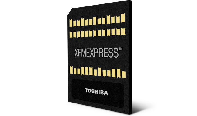
| 8:00a | Toshiba Introduces New Tiny NVMe SSD Form Factor
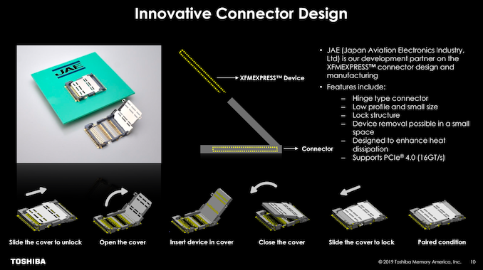
Today at Flash Memory Summit, Toshiba is debuting a new form factor for NVMe SSDs that is small enough to be a removable alternative to soldered-down BGA SSDs. The new XFMEXPRESS form factor allows for two or four PCIe lanes while taking up much less space than even the smallest M.2 22x30mm card size. The XFMEXPRESS card size is 18x14x1.4mm, slightly larger and thicker than a microSD card. It mounts into a latching socket that increases the footprint up to 22.2x17.75x2.2mm. For comparison, the standard sizes for BGA SSDs are 11.5x13mm with a PCIe x2 interface or 16x20mm with a PCIe x4 interface. XFMEXPRESS is intended to bring the benefits of replaceable storage to devices that would normally be stuck with soldered BGA SSDs or eMMC and UFS modules. For consumer devices this opens the way for aftermarket capacity upgrades, and for embedded devices that need to be serviceable this can permit smaller overall dimensions. Device manufacturers also get a bit of supply chain flexibility since storage capacity can be adjusted later in the assembly process. XFMEXPRESS is not intended to be used as an externally-accessible slot like SD cards; swapping out an XFMEXPRESS SSD will require opening up the case of the device it's installed in, though unlike M.2 SSDs the XFMEXPRESS socket and retention mechanism itself is tool-less.
XFMEXPRESS will allow for similar performance to BGA SSDs. The PCIe x4 host interface will generally not be the bottleneck, especially in the near future when BGA SSDs start adopting PCIe gen4, which the XFMEXPRESS connector can support. Instead, SSDs in these small form factors are often thermally limited, and the XFMEXPRESS connector was designed to allow for easy heat dissipation with a metal lid that can serve as a heatspreader. Toshiba partnered with Japan Aviation Electronics Industry Ltd. (JAE) to develop and manufacture the XFMEXPRESS connector. | |||||||||||||||||||||||||
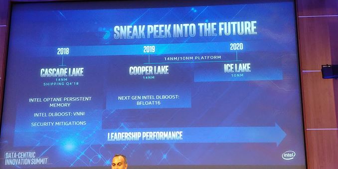
| 8:01a | Intel to Offer Socketed 56-core Cooper Lake Xeon Scalable in new Socket Compatible with Ice Lake
Today Intel is announcing some of its plans for its future Xeon Scalable platform. The company has already announced that after the Cascade Lake series of processors launched this year that it will bring forth another generation of 14nm products, called Cooper Lake, followed by its first generation of 10nm on Xeon, Ice Lake. Today’s announcement relates to the core count of Cooper Lake, the form factor, and the platform. | |||||||||||||||||||||||||
| 9:00a | The Fractal Design Ion+ 760P 80Plus Platinum PSU Review: A High-End PSU For the Mainstream Builder Fractal Design is releasing their new high-end PSU series, the Ion+. The series consists of four units with power outputs ranging from 560 to 860 Watts, all with impressive specifications overall. Today we'll be taking an in-depth look at the 760W model from this family, the aptly-named Ion+ 760P, and seeing first-hand how Fractal's new PSUs live up to the company's lofty claims. | |||||||||||||||||||||||||
| 3:30p | Samsung Unveils 6th Generation V-NAND Memory with Up to 136 Layers
Samsung on Tuesday introduced its sixth-generation V-NAND memory, which in a bid to further improve capacity and density, features over 100 active layers. To make V-NAND with over 100 layers viable from performance point of view, the company had to use new circuit design technology. The new memory features 10% lower latencies and consumes 15% lower amount of power when compared to Samsung's previous-generation V-NAND. Samsung’s 6th Generation V-NAND features up to 136 layers as well as charge trap flash (CTF) cells. The new memory uses one stack and does not use technologies like string stacking to build over 100 layers. In order to ensure minimal errors and low latencies, Samsung had to use a new speed-optimized circuit design. The latter enables the new 3D TLC 256 Gb chips to offer below 450 microseconds (μs) latency for write operations and below 45 μs for read operations, which is 10% faster when compared to 5th Generation V-NAND, according to Samsung. Meanwhile, the latest V-NAND also features lower power consumption than its predecessors. It is noteworthy that the new 256 Gb 136-layer V-NAND devices use 670 million holes, down from 930 million holes with the previous generation, which means that the new chips need fewer process steps and are easier to manufacture. What is important is that Samsung plans to use its 136-layer architecture with speed-optimized circuit design to build V-NAND devices with over 300 layers by mounting three of the current stacks on top of each other (thus tripling a chip’s capacity). Initially, Samsung will offer 256 Gb 3D TLC 136-layer V-NAND devices that will first be used for Samsung’s 250 GB SSDs. Later this year Samsung intends to release 512 Gb 136-layer V-NAND devices that will be used for other drives as well as eUFS storage solutions. Speaking of the 256 GB 6th Gen V-NAND SSD, it is important to point out that it uses Samsung’s new controller marked as the S4LR030/S94G4MW2.
Related Reading: Source: Samsung | |||||||||||||||||||||||||
| 5:00p | Rick Bergman Returns to AMD to Lead Computing & Graphics Business
AMD has announced that Rick Bergman had rejoined the company and will lead its Computing and Graphics business. Mr. Bergman’s focus will be high-performance PCs, gaming and semi-custom businesses. The return of the former executive emphasizes importance of gaming for AMD. Rick Bergman has a long history with GPU companies. In the late nineties he used to work at S3 Graphics and then joined ATI Technologies in 2001, where he served at various positions until 2006, when ATI was bought by AMD. From 2006 to 2011, he led AMD’s products group where he was responsible both for CPUs and GPUs. In 2011, Mr. Bergman joined Synaptics, where he served as CEO until recently and significantly transformed the company. Among the highlights of Rick Bergman’s career at AMD are the company’s highly-successful Radeon HD 4000 and HD 5000 families of products, the GCN architecture that was used by the company’s GPUs for years, as well as AMD’s ‘Fusion’ program that enabled the company to integrate its GPUs into its CPUs and eventually create high-performance SoCs for Microsoft’s and Sony’s game consoles. Rick Bergman is the latest addition to AMD’s graphics and gaming team. Last month AMD hired Frank Azor, a former head of Dell’s Alienware division, to head its gaming-related efforts. Meanwhile, Mr. Bergman brings both general management and semiconductor experience. Related Reading: Source: AMD | |||||||||||||||||||||||||
| 9:30p | Samsung Announces the Exynos 9825 SoC: First 7nm EUV Silicon Chip
This year’s Galaxy S10 has been in a bit of an odd situation: Although Samsung continued to dual-source its SoCs, using both its own Exynos 9820 SoC as well as Qualcomm’s Snapdragon 855, the phone found itself in the unusual situation of pitting 8nm silicon against 7nm silicon from TSMC. So although the new Exynos 9820 did fairly well in testing and improved a lot over the Exynos 9810, the chip seemingly still had disadvantages against the competition when it came to power efficiency, likely linked to its process technology disadvantages. On top of the power efficiency disadvantages, the chip also had a notable die area disadvantage versus the Snapdragon, coming in at 127mm² versus the smaller 73mm² competition. Samsung’s 7nm EUV process node was noted as having started mass production back in October of last year, although we’re not sure exactly which chip this was referring to, and we had hopes that it would be the chip for the S10 but alas it was not to be. This time around, Samsung is seemingly bridging the gap with the introduction of the new Exynos 9825 – a 7nm LPP refresh of the Exynos 9820.
The new chip very much looks like a die-shrink/mid-cycle refresh with largely the same IP generation as the 9820, still featuring Samsung’s M4 Cheetah cores as well as a Mali-G76 GPU. Samsung also doesn’t seem to have changed the clock frequencies of the chip very much: The M4 cores are still running at a peak frequency of 2.73GHz and the A55 cores also run at 1.95GHz. We do see a bump in the frequencies of the middle cores that goes up from 2.31GHz to 2.4GHz. On the GPU side, Samsung has also stuck with the same GPU configuration as with 9820, using a MP12 configuration of the G76. According to the company the 9825's GPU is clocked higher - so it will outperform its predecessor - however the company has yet to disclose specific clockspeeds. As for the integrated modem, Samsung has retained their Shannon 5000, a Category 20/13 modem. This modem has a peak download rate of 2 Gbps (with 8x carrier aggregration), while uploads top out at 316 Mbps. We had been wondering if Samsung would be able to squeeze in a 5G modem for this SoC, but it looks like it's just a bit too early for that. Instead, 5G can be accomplished by pairing the SoC with Samsung's 5G Exynos Modem 5100. The new chip is likely to be featured in the new Galaxy Note10 – Samsung will continue to use Snapdragon chips for some markets, and this could be an explanation for the new chip not having that big improvements on the part of the CPU complex as it’s aiming for performance parity with the Snapdragon. We also have to note that Samsung would have to invest the process improvements into improving power efficiency rather than raising performance. The chip reminds us of the Exynos 5430 from a few years ago which was also a process-shrink to the chip that ended up in the Galaxy S5, representing Samsung’s first 20nm silicon. That chip never ended up in the popular flagship products, but seemingly did serve a purpose as a pipe-cleaner and learning platform for the new process node. The new Exynos 9825 could end up in a similar situation, although being used in the Note10, it won’t nearly have an as long lifespan as we don’t expect it to power the Galaxy S11 next year. |

| << Previous Day |
2019/08/06 [Calendar] |
Next Day >> |