[Most Recent Entries] [Calendar View]
Wednesday, October 23rd, 2019
- ARM Details "Project Trillium" Machine Learning Processor Architecture
- Imagination Goes Further Down the AI Rabbit Hole, Unveils PowerVR Series3NX Neural Network Accelerator
- CEVA Announces NeuPro-S Second-Generation NN IP
- Cadence Announces Tensilica Vision Q7 DS
- Arm's New Mali-G77 & Valhall GPU Architecture: A Major Leap
- Arm Announces Mali D77 Display Processor: Facilitating AR & VR
- Arm Announces New Mali-D71 Display Processor and IP Blocks
- TSMC’s 5nm EUV Making Progress: PDK, DRM, EDA Tools, 3rd Party IP Ready
- TSMC: First 7nm EUV Chips Taped Out, 5nm Risk Production in Q2 2019
- TSMC Radically Boosts CapEx to Expand Production Capacities, To Reach $14B For 2019
- TSMC Announces Performance-Enhanced 7nm & 5nm Process Technologies
- Huawei Delays Launch of Foldable Mate X to Q4
- Huawei Launches the Mate X: Folding in a New Direction
- First Glimpse of Huawei Mate X: A Foldable 5G Phone
- Huawei CEO Richard Yu Q&A: “Politicians are Playing Games”
- Samsung’s Galaxy Fold Hits the US on September 27th
- GlobalFoundries Sues TSMC Over Patent Infringement; Apple, Qualcomm, Others Named Defendants
- TSMC Counter-sues GlobalFoundries: Accuses US Fab of Infringing Patents Across Numerous Process Nodes
- Apple and Qualcomm Bury the Hatchet; Sign New Patent and Chip Supply Agreements
- AMD Wins Patent Infringement Case Against Vizio & Others; Vizio Ordered To Cease Some TV Imports
- Samsung to Pay $400 Million for Infringing FinFET Patent
- Samsung Announces Exynos 980 - Mid-Range With Integrated 5G Modem
- Samsung Announces the Exynos 9825 SoC: First 7nm EUV Silicon Chip
- The Samsung Galaxy S10+ Snapdragon & Exynos Review: Almost Perfect, Yet So Flawed
- Samsung Announces 8nm Exynos 9820 With Tri-Group CPU Design
- Samsung Releases Exynos Modem 5100 - First Multi-Mode 5G Modem
| Time | Event | ||||||||||||||||||||||||||||
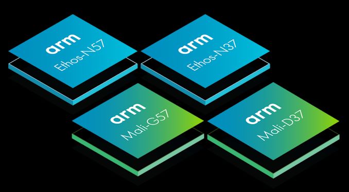
| 12:00a | Arm Announces New Ethos-N57 and N37 NPUs, Mali-G57 Valhall GPU and Mali-D37 DPU
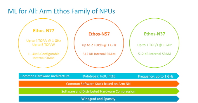
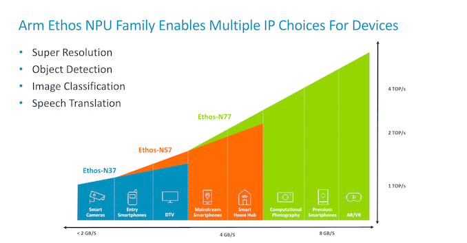
Today Arm is announcing four new products in its NPU, GPU and DPU portfolio. The company is branding its in-house machine learning processor IPs the Ethos line-up detailing more the existing N77 piece and also revealing the smaller N57 and N37 siblings in the family. To top things off, the company is also making ready its first mid-range GPU IP based on the brand-new Valhall architecture, the new Mali-G57. Finally, we’re seeing the release of a new mid-range DPU in the form of the Mali-D37. Introducing the Ethos NPU Family
Arm’s NPU IP offering was first announced early last year, detailing its architecture a few months later, and has been publicly been known until known just as “Project Trillium”. Arm at TechCon this year has officially branded the IP as the Ethos line-up, and the N77 has been the main product that’s been previously referred to as the Trillium codename. Microarchitecturally, the new branded Ethos-N77 now publicly changes its specs compared to what had been revealed last year by allowing for a configurable 1 to 4MB SRAM implementation, whilst last year it had been disclosed it would scale up to 1MB only. Arm explains that customers needed more memory bandwidth for processing these mesh networked NPUs, as DRAM bandwidth doesn’t scale up in the premium segment as fast as the core count does. The flagship IP offers up to 4TOPS processing power at 1GHz clock and has a respectable 5TOPS/W efficiency.
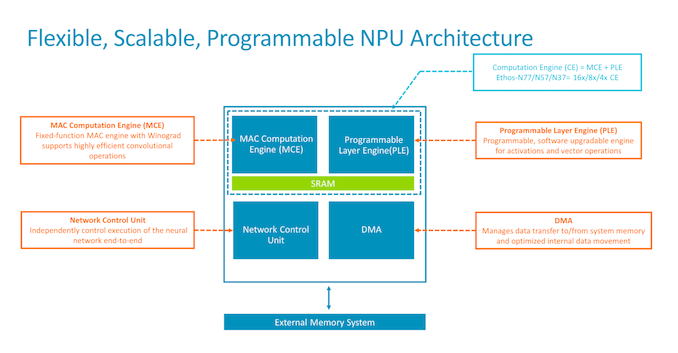
Arm is able to use the same building blocks across the different IPs. The NPUs all share the same MAC computation engine (MCE) and programmable layer engines (PLE). The MCE consists out of 128 MAC units, as disclosed last year, and is paired alongside a PLE. An MCE and PLE, plus SRAM, make up a computation engine (CE), and this is the scaling block that differs between the N77, N57 and N37, coming in 16x, 8x and 4x configurations in terms of the CE count.
The mid-range and low-end variants are being released a lot faster than other new IP technologies because Arm is seeing a lot more interest in doing ML in cost-constrained devices where every mm² of silicon is important. Particularly features like smartphone face unlocking or DTV resolution upscaling are becoming commodity features. The new NPUs have already been licensed and delivered to customers. Revealing the Mali-G57 - First Mid-range Valhall Based GPUEarlier this year, Arm had announced the new Valhall architecture in the new Mali-G77 that we’re expecting to see in SoCs next year. The new GPU architecture is a more major departure from the Bifrost based GPUs we’ve seen over the last three years as Arm has completely revamped its graphics ISA and computation microarchitecture.
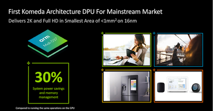
Today, Arm reveals that the company is adopting the new Valhall architecture in the mid-range, starting off with the new Mali-G57. We currently don’t have too many details on exactly what the finer microarchitecture configurations of the new GPU looks like, but we’re very likely looking at something that will be very similar to the G77, scaled down similar to how the G52 looked like compared to the G72. Improvements compared to a G52 with three execution engines per core (3EE) promise 1.3x better performance in a similar core configuration, 30% better energy efficiency, and 30% better silicon density (due to the better performance). Mali-D37 DPU - Bringing High-End Features To the Mid-RangeFinally, to wrap things up, Arm is now bringing to market a new mid-range DPU in the form of the Mali-D37.
The new IP is based on the “Komeda” architecture which was first introduced in the Mali-D71 and its follow-up, the Mali-D77 announced this year. Then new DPU targets resolutions of 2K and FHD and promises to take up only <1mm² on 16nm. Related Reading | ||||||||||||||||||||||||||||
| 8:00a | The AUKEY KM-G3 RGB Mechanical Keyboard Review: A Basic Budget Mechanical Keyboard Today we are taking a look at the KM-G3 RGB Mechanical keyboard from AUKEY, a Chinese manufacturer. Designed as an entry-level mechanical keyboard, AUKEY engineered the KM-G3 to offer mechanical switches and RGB lighting at a significantly lower price than the competition. There aren't any advanced features to speak of, but as a result AUKEY sells the keyboard for just $65, and it is often on sale for even less than that. | ||||||||||||||||||||||||||||
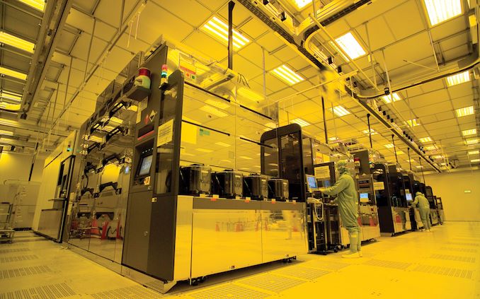
| 10:00a | TSMC: 5nm on Track for Q2 2020 HVM, Will Ramp Faster Than 7nm
TSMC’s 5 nm (N5) manufacturing technology is projected to provide significant benefits when it comes to performance, power, and area scaling, which is why the contract maker of semiconductors expects a tangible number of its customers to adopt this process. And, with a forecast for aggressive demand paired with some early preparation in installing new equipment, TSMC believes that its N5 technology will ramp even quicker than its 7 nm (N7) process. In a bid to boost its production capacities, TSMC recently increased its capital expenditures for 2019 from $10 billion - $11 billion to $14 billion - $15 billion. TSMC is particularly invested in buying equipment for its cutting-edge nodes, such as ASML’s Twinscan NXE step-and-scan systems for processes that use extreme ultraviolet lithography (EUVL) for select layers. At present, TSMC’s Fab 15 is making SoCs using N7+, whereas its Fab 18 (the first phase of equipment move-in was completed in March 2019) is on-track to produce N5 chips in high volume starting Q2 2020. The new tools that will be bought in the coming months are expected to be installed in 2020 and this is when the company will be able to quickly ramp production of chips using its N7, N7+, N7P, N6, N5, and N5P process technologies. The company is confident that it will have a very high market share with its 5 nm nodes. C.C. Wei, vice chairman and CEO of TSMC, said the following:
The key difference between N5 and its predecessors that use EUVL is that it is designed to use EUVL on up to 14 layers (up from four and five in case of N7+ and N6). So the ramp of N5 will increase usage of the latest equipment, and to some degree will demonstrate whether EUV tools and ecosystem is ready for prime time or not. Right now, TSMC seems to be very optimistic about EUVL. The light sources it uses offer output power of more than 250 Watts and reach target goals for availability. The company also produces its own pellicles and takes into account characteristics of currently available photoresists. Mr. Wei said the following:
Related Reading: Source: TSMC | ||||||||||||||||||||||||||||
| 12:30p | The Foldable Huawei Mate X: Coming to China on November 15th for ~$2074
Foldable smartphones from Huawei and Samsung attracted quite a lot of public attention at Mobile World Congress early this year, but launches were delayed as companies had to polish the technology. Samsung’s Galaxy Fold has since been released into the market in select countries (Ian: my local EE store has sold a dozen or so), whereas the Mate X, its rival from Huawei, is coming later. As it turns out, Huawei plans to launch its Mate X in China on November 15. The foldable smartphone, which is powered by the HiSilicon Kirin 980 SoC (paired with 8 GB of RAM and 512 GB of storage), the Balong 5000 5G modem, and features an 8-inch foldable display with a 2480x2200 resolution and a 9:8 aspect ratio, will cost ¥16,999. This translates into a ~$2074 price in the US.
It is not completely clear when Huawei’s Mate X is set to arrive to other markets (if at all) and what kind of software will it have pre-installed. Considering how expensive the smartphone is, selling it potentially without applications from Google and other US-based vendors may not be a good idea in non-Chinese markets
In addition to revealing the launch date of the Mate X, Huawei also said today that it plans to release a refined version of the foldable smartphone, the Mate Xs, on the HiSilicon Kirin 990 5G SoC. It has a built-in 5G modem, and is set to come to China in March. It is unknown how much will the unit cost and whether it will be available outside of China. Related ReadingSources: Engadget China (via Engadget), VMall (via GSMArena) | ||||||||||||||||||||||||||||
| 5:45p | Intel Files Antitrust Suit Against SoftBank-Controlled Firm Over Patent Aggregation
Intel this week filed an lawsuit against Fortress Investment Group, a patent assertion entity controlled by SoftBank. Responding to a series of patent infringement lawsuits that Fortress has brought against Intel in recent years, Intel's latest lawsuit accuses Fortress of engaging in anticompetitive behavior, alleging that Fortress stockpiled technology patents in order to patent troll Intel. As a result, Intel is asking the courts to declare Fortress’s patent aggregation business practice as unlawful, and essentially unwind Fortress's operations. In the recent years IP aggregation with an aim to enforce patents and receive royalties has developed into a business in and of itself. This has lead to the rise of firms known as patent assertion entities (PAEs) — or commonly called patent trolls — who acquire a large number of patents from various companies and then license them (often in package deals) to high-tech companies who are developing actual products. Through a network of PAEs that Fortress controls, it owns more than a 1,000 U.S. technology patents. Among these are patents originally granted to NXP Semiconductor, giving Fortress a fairly deep collection of chip design patents to enforce. As a result, Fortress (and other PAEs it controls) have previously filed lawsuits against Intel claiming that virtually all CPUs from the company produced since 2011 illegally use the NXP IP. While Intel is not contesting the validity of the patents themselves, the company is contesting the legality of Fortress's actions with those patents. In its suit, Intel claims that Fortress's patent aggregation business violates Sections 1 and 2 of the Sherman Antitrust Act, as well as Sections 4 and 7 of the Clayton Act (an antitrust law covering unethical business practices), with Intel asking the U.S. District Court for the Northern District of California to act and remedy the situation. Overall, Intel is asking the court to declare Fortress’s patent aggregation business practice as unlawful, declare all patents obtained in violation of the laws as unenforceable, declare all patent contracts and agreements entered into violation of laws as illegal, and transfer all of the claimed patents back to the transferors. Ultimately, Intel's case rests on the idea that patent enforcement actions by PAEs do not necessarily help to drive innovation by inventors, but rather they hurt manufacturers. As such, what's being called into question is how those patents are being used and enforced, rather than their technical validity. Especially, as Intel insinuates, that Fortress's entire business model is based around the idea of parlaying patents – specifically looking to profit from the spread between what Fortress pays for the patent and what they think they can get companies to settle for out of court (rather than spending even more money defending them in court). Intel for its part is hardly new at fighting against patent trolls. However, the major complication in this case is that Fortress is a SoftBank business – having been acquired for $3.3 billion back in 2017 – meaning it has the backing of the Japanese conglomerate. So Fortress is far more well heeled than the typical PAE, and SoftBank itself is already a natural competitor to Intel, as it also owns Arm. Here is what Intel said in its antitrust suit titled ‘Intel Corporation v. Fortress Investment Group LLC et al’ (5:2019cv06856):
Related Reading: Source: Reuters, USCourts.Gov | ||||||||||||||||||||||||||||
| 6:00p | Samsung Announces Exynos 990: 7nm EUV, M5, G77, LPDDR5 Flagship SoC alongside Exynos 5123 5G Modem Today Samsung unexpectedly announced the brand new Exynos 990 chipset – likely to be Samsung’s flagship SoC for 2020, employing the newest IP and offering the newest features on the 7nm EUV manufacturing node. The chip closely follows the release of the Exynos 980 earlier in September, and both new silicon chips bring with them 5G connectivity alongside their new product naming scheme.
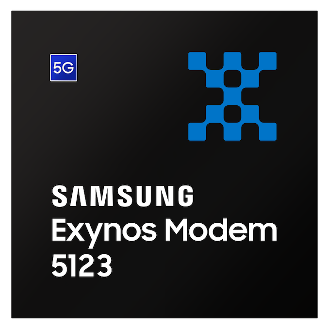
Starting off with the new CPU complex, Samsung seemingly is continuing with their custom CPU designs for this generation, and we’re seeing the deployment of the new Exynos M5 microarchitecture. Samsung quotes that the new design is 20% faster than the Exynos M4 in the 9820 – a bit of a conservative figure given the larger process node improvement. The new CPU will have to compete against the next generation Snapdragon flagship which most likely will come with Cortex-A77 derived cores which promises 23-30% IPC increases – unless that chip comes with clock degradations, the new M5 will have a hard time competing. Samsung has upgraded the middle core from the Cortex A75 in the previous generation a newer Cortex A76 design, which should provide a more significant performance uplift in every-day workloads. Finally, we continue to see Cortex A55 cores as the little efficiency cores. Samsung doesn’t disclose the clock frequencies of any of the CPU clusters, but advertises that the overall improvement of the new tri-cluster is 13%. The Exynos 990 sees a big GPU upgrade in the form of the new Mali-G77 in an MP11 configuration. The new Valhall architecture promises to be a very large performance jump for Arm’s GPU IP, and it looks like the new Exynos will be amongst the first chipsets to employ the new GPU family. Samsung press release claims we’ll see performance uplifts of up to 20%, or power efficiency gains of up to 20%. The increase seems quite meagre given the process improvement as well as the new GPU architecture, it seems very unlikely Samsung will be able to catch up to Apple’s newest chipsets – and Qualcomm is expected to have a big generational jump as well. One fundamental change that the Exynos 990 brings with itself is the transition from LPDDR4X memory to LPDDR5 memory. This allows the new chipset to increase the memory controller frequency from 2093 MHz to 2750MHz and we’re also expecting the new DRAM technology to bring power efficiency gains to the table. Samsung discloses that the chip comes with a dual-core NPU and a new DSP which can perform over 10 TOPs in computational throughput – it’s not exactly clear here if Samsung is referring to the DSP’s capability or the combined capabilities of the NPU and DSP. The Exynos 9820’s NPU had a throughput of 1.86TOPs. Finally, what’s odd here is the chip’s connectivity capabilities: Samsung doesn’t list the Exynos 990 as having modem capabilities which might point out that we’re maybe looking at a pure application processor this generation. Instead of an integrated modem, Samsung is advertising the new Exynos Modem 5123 as a new discrete chipset:
The new modem iterates on the Exynos Modem 5100 used this year: It’s still a complete multi-band solution supporting everything from 2G to 5G sub-6 as well as mmWave, however Samsung has massively upgraded the new chip’s maximum throughput. In regular 4G LTE, the new chip now supports downlink speeds of up to 3Gbps while offering 422Mbps upload. In 5G sub-6, we’re seeing 5.1Gbps downloads, and 7.35Gbps in mmWave networks. The chip’s speeds are enabled by up to 8x carrier aggregation and a new higher-order 1024 QAM, which is as far as we know, the first modem to be announced with such capabilities. Samsung’s choice of going with a discrete 5G modem this generation seems to be related to the economics of the new silicon: The new 5G modems are still quite large in die size, although the Exynos Modem 5100 was amongst the smallest at 56.03mm². Still, both the new modem as well as the Exynos 990 are manufactured on Samsung’s 7nm EUV node, and separating the two into discrete chips likely makes sense at this point in time in order to offer more flexibility and to increase manufacturing yield. One question which remains open, is whether Samsung will be opting to pair the Exynos 990 with a different modem than the 5123. Still, it’s unlikely that we’ll see any pairing with a 4G modem, meaning all Exynos flagship devices next year will have 5G support. Samsung says we’ll see the Exynos 990 in mass production by the end of the year, and we’re likely have the Galaxy S11 being powered by the new piece. Related Reading: |


| << Previous Day |
2019/10/23 [Calendar] |
Next Day >> |