[Most Recent Entries] [Calendar View]
Thursday, February 27th, 2020
- BIOSTAR Brings Windows 7 To Intel's B365 Platform
- The Biostar A10N-8800E Motherboard Review: Carrizo in 2019?!
- BIOSTAR Adds Windows 7 Support To Some Intel and AMD Motherboards
- The Biostar X470GTN Motherboard Review: AM4 ITX Revisited
- The Biostar X370GTN Mini-ITX Motherboard Review: AM4 Goes Tiny
- Mining Can Be Fashionable? Biostar Wants to Sell Millenials its New iMiner Systems
- Samsung Ships First Commercial Embedded MRAM (eMRAM) Product
- MRAM Developer Day, GlobalFoundries Keynote Live Blog
- Everspin Begins Production of 1Gb STT-MRAM
- GlobalFoundries Teams Up with Singapore University for ReRAM Project
- CES 2020: ZOTAC’s Inspire Studio SFF PCs for Creators w/ 8-Core CPU & GeForce RTX
- ZOTAC Expands MEK Lineup with MEK Mini and MEK Ultra
- Zotac at CES 2018: ZBOX MAGNUS Upgraded with Coffee
- Sapphire Announces Two 4x4 AMD Ryzen Embedded Motherboards
- Ryzen UCFF-palooza: Multiple PC Makers Now Shipping AMD Ryzen Embedded Systems
- SimplyNUC Unveils Sequoia: AMD Ryzen V-Series-Based UCFF PC
- Sapphire Unveils FS-FP5V: AMD Ryzen Embedded Mini-STX Motherboard
- GlobalFoundries Stops All 7nm Development: Opts To Focus on Specialized Processes
- GlobalFoundries Weds FinFET and SOI in 14HP Process Tech for IBM z14 CPUs
- GlobalFoundries to Expand Capacities, Build a Fab in China
- GlobalFoundries and Chinese Authorities Reconsider Plans
- GlobalFoundries Enables Connectivity IP: New RF SOI and Ensigma BLE on 22FDX
| Time | Event | ||||||||||||||||||||||||||||||||||||||||||||||||||||||||||||
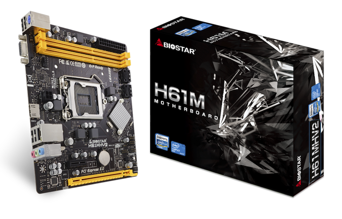
| 4:45a | 2011 is Calling: Biostar Relaunches H61 Chipset in 2020
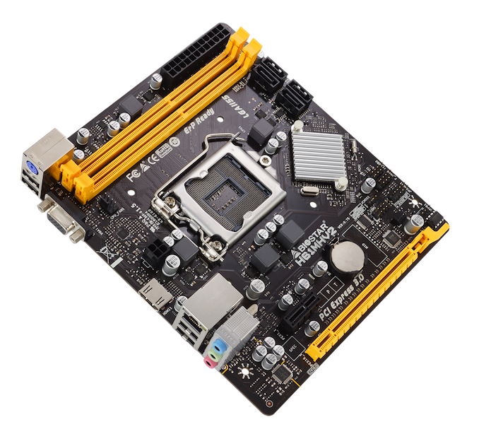
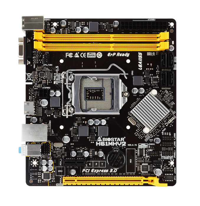
Almost a decade ago, with the launch of Intel’s Sandy Bridge processors, came the H61 chipset. Compared to the high-end P67 and Z68 models, the idea behind H61 is that it was cheap, and it was long-life. At a time when low power embedded Atom CPUs still didn’t have enough power, H61 was there to be equipped with one of Intel’s new-fangled Core processors, with the systems that designed for it destined to last a couple of decades. We’re now 9 years into that life cycle, and Biostar deems it necessary to create a new H61 design for the new decade. We’re getting to a time now where the cheaply made H61 boards of yesteryear are starting to go pop. When you save a tenth of a cent on capacitors, eventually you get to an age where one doesn’t work and the magic smoke appears. Systems which are built on these have two options: replace the failed component, or upgrade completely. What may surprise some people is that the easiest option is always the first one: replace the broken component. By replacing hardware like-for-like, the system is already set up and ready to go when the new part is installed. If a customer decided to go a different route with a Gemini Lake, sure there might be more performance, but then the signalling standards have changed, the memory has changed, the capabilities of the CPU have changed, etc. By introducing its new H61 motherboard into the mix, the H61MHV2, Biostar is hoping to capitalize on a decade of experience with newer high performance motherboards, and the ability to play the supply chain for the best deals. As a result of a decade of advancement, elements such as the Ethernet have been updated – up from a 100 Mbps chip to a 1 Gbps chip. DDR3-1600 slots are now in line with the rear IO panel to help airflow, and the socket has changed orientation as well. We should expect to see a few updates perhaps in the BIOS and software as well.
The Biostar H61MHV2 doesn’t quite meet the strict requirements for a mini-ITX board, being one slot longer – presumably for those customers that need the extra PCIe x1 slot. The main PCIe slot is actually PCIe 3.0 x16, but only when a Core i5 or Core i7 Ivy Bridge processor is used. This motherboard supposedly supports all the way up to the Core i7-3770K. The SATA ports are only SATA 3 Gbps, half the speed of modern SATA connections, and there are no USB 3.0 ports here. Audio is the simplest Realtek ALC662 chip that money can buy, and the same one used by the Biostar IH61MF-Q5, which the company states is what this new board is replacing. Over the IH61MF-Q5, the only spec-sheet difference between the two seems to be the HDMI output, as well as support for Windows 10. In a visual inspection between the two, we can see some of the layout has changed as well. Users buying this new H61 board, we expect, are just going to be replacing their original $50 designs with something similar. However kudos to anyone building a new system with it. 2011 was the year that William and Kate got married, Steve Jobs passed, and Thailand got flooded so a lot of PC components got more expensive. Hopefully 2020 isn’t a repeat of similar news.
We have asked Biostar’s PR agency for pricing, and will update the article when we get it. Related Reading | ||||||||||||||||||||||||||||||||||||||||||||||||||||||||||||
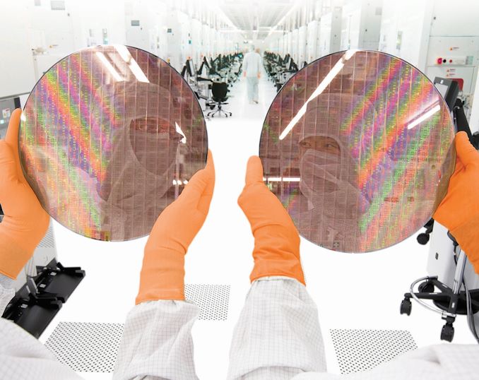
| 8:00a | GlobalFoundries' 22FDX with MRAM is Ready
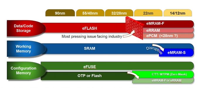
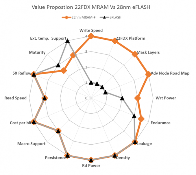
GlobalFoundries on Thursday said that it had completed development of its 22FDX (22 nm FD-SOI) technology with embedded magnetoresistive non-volatile memory (eMRAM). The technology can be used for a variety of applications, including automotive, industrial-grade MCU, and Internet-of-Things (IOT). Several clients of GlobalFoundries are ready to tape out their first 22FDX chips with eMRAM this year. eMRAM provides a number of advantages when compared to eFlash (which is widely used today) for chips that need relatively high-capacity onboard storage, including higher performance and endurance, but want it all in a single silicon die. MRAM does not involve electric charges or current flows, instead, it uses magnetic storage elements and relies on reading the magnetic anisotropy (orientation) of two ferromagnetic films separated by a thin barrier. The method does not require an erase cycle before writing data, which means additional performance. Furthermore, MRAM can be produced using modern process technologies and has a very high endurance. The technology has some downsides, which will be eventually addressed by fabrication processes that use ReRAM, but GlobalFoundries and Samsung Foundry see a huge potential in in MRAM for the vast majority of applications.
GlobalFoundries’s says that test chips produced using its 22FDX with eMRAM process technology have demonstrated a 100,000-cycle endurance and a 10-year data retention across the -40°C to 125°C operating temperatures with ECC-off mode. Furthermore, the company’s eMRAM test product can pass standard reliability test, including LTOL (168 hours), HTOL (500 hours), and 5x solder reflows with failure rate < 1 ppm. In addition, GlobalFoundries has addressed concerns about magnetic immunity (of a product that relies on magnetic storage elements). The company says that its test 40 Mb product demonstrated a stand-by magnetic immunity of ~ 600 oersted at 105°C for 10 years (which means no read failures), whereas its active-mode magnetic immunity was ~500 oersted.
GlobalFoundries offers silicon-validated MRAM macros featuring capacities from 4 Mb to 48 Mb that can be used for various designs. At present, the technology has been qualified for AEC-Q100 Grade 2 designs with a -40°C to 105°C temperature range. Next year, the company will offer a version of the process qualified for AEC-Q100 Grade 1 temperatures (-40°C to 125°C). GlobalFoundries produces chips using its 22FDX technology at its 300-mm Fab 1 in Dresden, Germany. The same production facility will handle production of devices made using the company’s 22FDX with eMRAM. Mike Hogan, senior vice president and general manager of automotive and industrial multi-market at GlobalFoundries said the following:
Related ReadingSource: GlobalFoundries | ||||||||||||||||||||||||||||||||||||||||||||||||||||||||||||
| 9:00a | Testing a Chinese x86 CPU: A Deep Dive into Zen-based Hygon Dhyana Processors In 2016, through a series of joint ventures and created companies, AMD licensed the design of its first generation Zen x86 processors to be sold into China. The goal of this was two-fold: China wanted a ‘home grown’ solution for high-performance x86 compute, and AMD at the time needed a cash injection. The outcome of this web of businesses was the Hygon Dhyana range of processors, which ranged from commercial to server use. Due to the Zen 1 design on which it was based, it has been assumed that the performance was in line with Ryzen 1000 and Naples EPYC, and no-one in the west has publicly tested the hardware. Thanks to a collaboration with our friend Wendell Wilson over at YouTube channel Level1Techs, we now have the first full review of the Hygon CPUs. | ||||||||||||||||||||||||||||||||||||||||||||||||||||||||||||
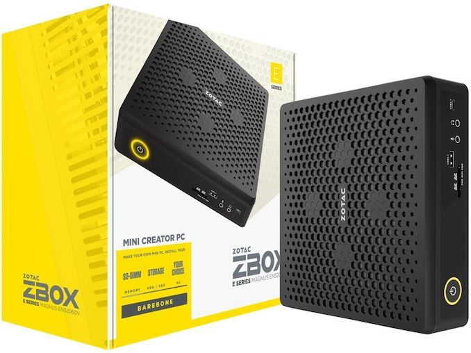
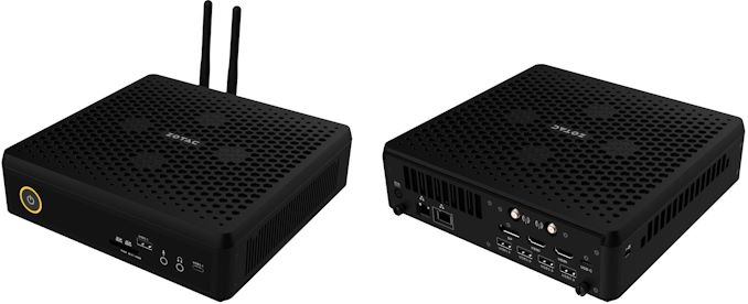
| 10:30a | ZOTAC Unveils Zbox Magnus EN52060V: A UCFF PC with GeForce RTX 2060 & 2.5 GbE
Zotac has quietly added a new mainstream gaming barebones system into its lineup of ultra-compact systems. With its quad-core Intel processor and NVIDIA’s GeForce RTX 2060 graphics card, the new Zbox Magnus EN52060V promises the performance of a mid-range mobile PC for gamers, but at a lower price and with all advantages that a desktop can offer. The new barebones system comes in ZOTAC’s regular 2.65-liter Zbox Magnus EN chassis, which is just 62.2 mm (2.45 inches) tall. The Zbox Magnus EN52060V UCFF PC barebones is based on Intel’s quad-core Core i5-9300H processor (4C/8T, 2.40 GHz – 4.10 GHz, 45 W) accompanied by NVIDIA’s GeForce RTX 2600 discrete GPU with 6 GB of GDDR6 memory. The system can be equipped with up to 32 GB of DDR4-2600 memory, an M.2-2280 SSD with a PCIe 3.0 x4 or SATA interface, and a 2.5-inch storage device.
The barebones system uses a mobile processor in an FCBGA1440 packaging, so it cannot be upgraded. Meanwhile, it is unclear whether the system uses a soldered-down discrete GPU, or an MXM module that could theoretically be upgraded. When it comes to connectivity, the Zbox Magnus EN52060V supports a Wi-Fi 6 + Bluetooth 5 adapter, two RJ-45 cores (2.5 GbE + GbE), two USB 3.1 Type-C connectors, four USB 3.0 Type-A ports, four display outputs (a DP 1.4, two HDMI 2.0b, one USB-C), an SD card reader, and two 3.5-mm audio jacks for headphones and a microphone.
ZOTAC already lists its Zbox Magnus EN52060V on its website, so it is reasonable to expect it to become available shortly. As for pricing, while Zotac has not announced anything at this time, based on its specifications we expect that this should end up the cheapest of Zotac's GeForce RTX-equipped Magnus EN-series PCs. Related Reading: Source: ZOTAC (via Hermitage Akihabara) | ||||||||||||||||||||||||||||||||||||||||||||||||||||||||||||
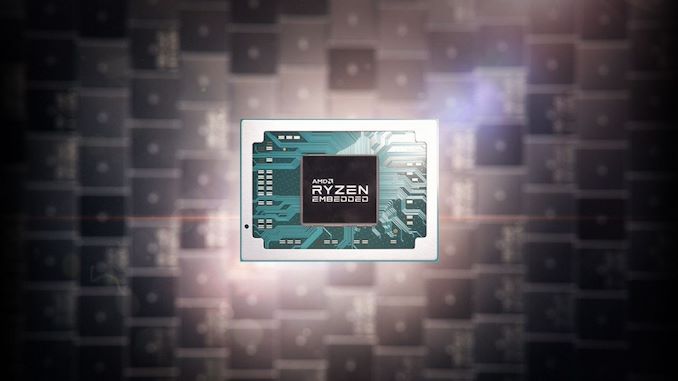
| 12:00p | AMD Launches Ultra-Low-Power Ryzen Embedded APUs: Starting at 6W
While it doesn't get the same attention as their high-profile mobile, desktop, or server CPU offerings, AMD's embedded division is an important fourth platform for the chipmaker. To that end, this week the company is revealing its lowest-power Ryzen processors ever, with a new series of embedded chips that are designed for use in ultra-compact commercial and industrial systems. The chips in question are the AMD Ryzen Embedded R1102G and the AMD Ryzen Embedded R1305G SoCs. These parts feature a 6 W or a configurable 8 W - 10 W TDP, respectively. Both SoCs feature two Zen cores with or without simultaneous multithreading, AMD Radeon Vega 3 graphics, 1 MB L2 cache, 4 MB L3 cache, a single channel or a dual-channel memory controller, and two 10 GbE ports.
AMD says that a low TDP and reduced number of supported DIMMs (in case of the R1102G) enable system makers to simplify their designs and make them cheaper as compared to machines that run AMD's higher performing and higher TDP Ryzen Embedded processors. AMD’s first customers to use the Ryzen Embedded R1102G and the Ryzen Embedded R1305G SoCs will be Kontron, which has a scalable D3713-V/R Mini-ITX platform, and Simply NUC, which has its Red Oak miniature PC. Other makers may get a 4x4 motherboard from Sapphire based on AMD's new Ryzen Embedded R1000-series APUs. Both ultra-low-power AMD Ryzen Embedded APUs will be available for the next 10 years, meaning availability will stretch all the way till 2030. Related Reading: Source: AMD | ||||||||||||||||||||||||||||||||||||||||||||||||||||||||||||
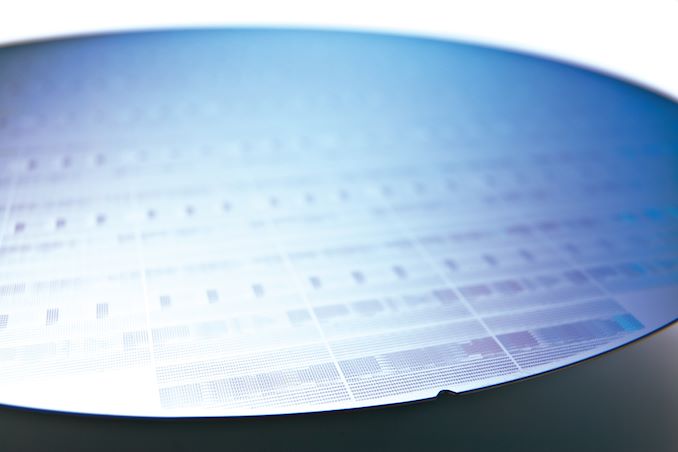
| 5:30p | A Big Bet on SOI: GlobalFoundries Preps Another Supply Agreement for 300mm SOI Wafers
Having dropped out of the race for leading-edge manufacturing technologies in order to focus on specialty fabrication processes, GlobalFoundries has pinned some big hopes in manufacturing RF-SOI chips for various 5G applications, as well as FD-SOI chips for low-power devices. This week the company signed a memorandum of understanding (MOU) with GlobalWafers Co. (GWC) to develop a long-term supply contract for 300 mm SOI wafers, GloFo's second long-term SOI wafers supply agreement (WSA) in less than a year. Once primarily used to build leading-edge processors, silicon-on-insulator (SOI) technology is used today for a wide variety of applications, including those that need an ultra-low power consumption (SoCs and MCUs for IoT applications), high voltages (analog/mixed signal), or high resistivity (4G and 5G front-end modules [FEMs] for smartphones). All of these are made using so-called specialty manufacturing technologies, and to that end they are of tremendous interest for GlobalFoundries. Meanwhile, considering the rise of 5G and IoT, RF-SOI and FD-SOI are the most promising technologies when it comes to producing the necessary chips in high volumes.
Nowadays, GlobalFoundries operates seven fabs: four 300-mm fabs (including the Fab 10 in East Fishkill, New York) and three 200-mm fabs. The company’s largest 300-mm Fab, Fab 1, is used exclusively to make SOI products, Fab 7 in Singapore uses both bulk and SOI technologies, and Fab 10 can also process wafers using SOI-based processes. In addition, GlobalFoundries is building another 300-mm fab in Chengdu, China, which will also be used to make chips using its 22FDX technology. Finally, the foundry’s 200-mm facilities can all use SOI wafers as well. Being the largest consumer of SOI wafers in the world, GlobalFoundries sources 200-mm and 300-mm substrates from both Soitec, the world’s largest producer of SOI wafers, as well as GlobalWafers Co. In fact, in just the last year GloFo and Soitec signed a multi-year 300-mm SOI wafer supply agreement, which builds upon a WSA signed in 2017. As it turns out, GlobalFoundries needs even more 300-mm SOI wafers for its advanced RF SOI technologies, so the company is going as far as agreeing to help GWC ‘significantly expand’ its SOI wafer manufacturing capacity as part of the new contract. GlobalFoundries, Soitec, and GlobalWafers Co. naturally do not disclose how many wafers are consumed by the chip maker. Regardless, it looks like we are talking about a significant expansion of SOI usage at GlobalFoundries. Bami Bastani, senior vice president for mobile and wireless infrastructure at GlobalFoundries:
Tom Weber, senior vice president and chief procurement officer at GlobalFoundries said the following:
Related Reading: Source: GlobalFoundries | ||||||||||||||||||||||||||||||||||||||||||||||||||||||||||||


| << Previous Day |
2020/02/27 [Calendar] |
Next Day >> |