[Most Recent Entries] [Calendar View]
Thursday, July 2nd, 2020
| Time | Event |
| 9:00a | The Intel Lakefield Deep Dive: Everything To Know About the First x86 Hybrid CPU For the past eighteen months, Intel has paraded its new ‘Lakefield’ processor design around the press and the public as a paragon of new processor innovation. Inside, Intel pairs one of its fast peak performance cores with four of its lower power efficient cores, and uses novel technology in order to build the processor in the smallest footprint it can. The new Lakefield design is a sign that Intel is looking into new processor paradigms, such as hybrid processors with different types of cores, but also different stacking and packaging technologies to help drive the next wave of computing. With this article, we will tell you all you need to know about Lakefield. |
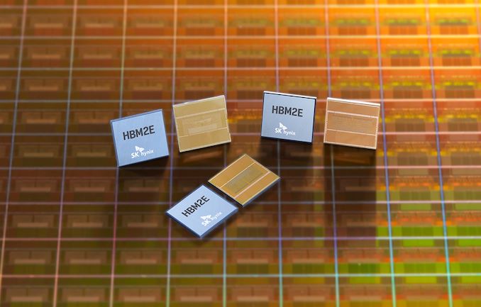
| 10:00a | SK Hynix: HBM2E Memory Now in Mass Production
Just shy of a year ago, SK Hynix threw their hat into the ring, as it were, by becoming the second company to announce memory based on the HBM2E standard. Now the company has announced that their improved high-speed, high density memory has gone into mass production, offering transfer rates up to 3.6 Gbps/pin, and capacities of up to 16GB per stack. As a quick refresher, HBM2E is a small update to the HBM2 standard to improve its performance, serving as a mid-generational kicker of sorts to allow for higher clockspeeds, higher densities (up to 24GB with 12 layers), and the underlying changes that are required to make those happen. Samsung was the first memory vendor to ship HBM2E with their 16GB/stack Flashbolt memory, which runs at up to 3.2 Gbps in-spec (or 4.2 Gbps out-of-spec). This in turn has led to Samsung becoming the principal memory partner for NVIDIA’s recently-launched A100 accelerator, which was launched using Samsung’s Flashbolt memory. Today’s announcement by SK Hynix means that the rest of the HBM2E ecosystem is taking shape, and that chipmakers will soon have access to a second supplier for the speedy memory. As per SK Hynix’s initial announcement last year, their new HBM2E memory comes in 8-Hi, 16GB stacks, which is twice the capacity of their earlier HBM2 memory. Meanwhile, the memory is able to clock at up to 3.6 Gbps/pin, which is actually faster than the “just” 3.2 Gbps/pin that the official HBM2E spec tops out at. So like Samsung’s Flashbolt memory, it would seem that the 3.6 Gbps data rate is essentially an optional out-of-spec mode for chipmakers who have HBM2E memory controllers that can keep up with the memory. At those top speeds, this gives a single 1024-pin stack a total of 460GB/sec of memory bandwidth, which rivals (or exceeds) most video cards today. And for more advanced devices which employ multiple stacks (e.g. server GPUs), this means a 6-stack configuration could reach as high as 2.76TB/sec of memory bandwidth, a massive amount by any measure. Finally, for the moment SK Hynix isn’t announcing any customers, but the company expects the new memory to be used on “next-generation AI (Artificial Intelligence) systems including Deep Learning Accelerator and High-Performance Computing.” An eventual second-source for NVIDIA’s A100 would be among the most immediate use cases for the new memory, though NVIDIA is far from the only vendor to use HBM2. If anything, SK Hynix is typically very close to AMD, who is due to launch some new server GPUs over the next year for use in supercomputers and other HPC systems. So one way or another, the era of HBM2E is quickly ramping up, as more and more high-end processors are set to be introduced using the faster memory. |
| << Previous Day |
2020/07/02 [Calendar] |
Next Day >> |