[Most Recent Entries] [Calendar View]
Thursday, August 13th, 2020
| Time | Event |
| 9:00a | The Intel Xe-LP GPU Architecture Deep Dive: Building Up The Next Generation As part of today’s Intel Architecture Day, Intel is devoting a good bit of its time to talking about the company’s GPU architecture plans. Though not a shy spot for Intel, per-se, the company is still best known for its CPU cores, and the amount of marketing attention they’ve put into the graphics side of their business has always been a bit weaker as a result. But, like so many other things at Intel, times are changing – not only is Intel devoting ever more die real estate to GPUs, but over the next two years they are transitioning into a true third player in the PC GPU space, launching their first new discrete GPU in several generations. |
| 9:01a | Intel’s 11th Gen Core Tiger Lake SoC Detailed: SuperFin, Willow Cove and Xe-LP At the start of the year, Intel ‘foolishly’ handed me a wafer of its next generation Tiger Lake processors, as the moment it came into my hands I attempted to make a very quick exit. In my time with the wafer, we learned that this new 10nm laptop-focused processor had four cores, used Intel’s next generation Xe graphics architecture, and would set the stage at the end of the year as the cornerstone of Intel’s mobile processor offerings. As part of Intel’s Architecture Day 2018 a couple of days ago, the company went into detail about what makes Tiger Lake the true vehicle for 10nm, and why customers will want a Tiger Lake device. |
| 9:10a | Intel Previews 4-Layer 3D XPoint Memory For Second-Generation Optane SSDs
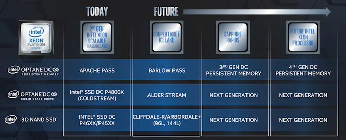
As part of Intel's Architecture Day 2020 presentations, Raja Koduri spent a bit of time talking about the status of their Optane products. Most of it was a recapitulation of details Intel has previously shared. The two important Optane product updates planned for this year are the Barlow Pass second-generation Optane DC Persistent Memory Modules (DCPMM) and the Alder Stream second-generation Optane NVMe SSDs.
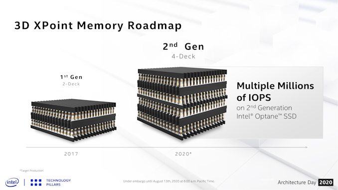
Intel has been teasing their Alder Stream second-generation Optane SSDs since last fall, with promises of off-the-charts performance increases. They've confirmed that Alder Stream will be using second-generation 3D XPoint memory, which moves from two to four layers ("decks" in Intel's slides), making this the first test of the vertical scaling potential of 3D XPoint technology. This combined with with a new SSD controller supporting PCIe 4.0 will enable "multiple millions" of IOPS, more than doubling the throughput of current Optane SSDs. Raja also mentioned that they've made optimizations to single-sector reads, so 4kB QD1 random read latency should be improved a bit as well—but this latency is already substantially limited by the latency of PCIe and NVMe command processing. Intel recently stated that they have not yet decided where to spun up their own volume manufacturing of 3D XPoint memory, so the second-gen 3D XPoint used in Alder Stream will still be manufactured by former partner Micron and purchased by Intel.
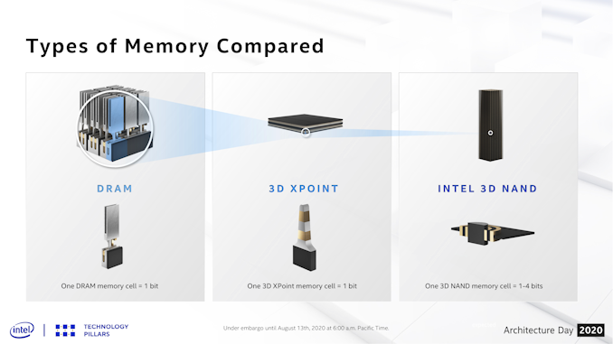
DRAM, 3D XPoint and 3D NAND memories, approximately to scale Barlow Pass has already launched alongside Cooper Lake Xeons and will be the Optane DCPMM product for Ice Lake Xeons as well. Intel claims an average of 25% higher bandwidth for Barlow Pass than the initial Apache Pass modules for Cascade Lake Xeons. The fine print in Intel's slides indicates that the 4-deck 3D XPoint memory used in Alder Stream Optane SSDs is not yet in mass production. That and the omission of any mention of the second-generation, 4-deck 3D XPoint memory in the context of Optane DCPMM products all but confirms that Barlow Pass is still using first-gen 3D XPoint memory. This is consistent with the more modest 25% bandwidth increase as compared to the drastic improvements due to arrive with the Alder Stream SSDs. It appears that Ice Lake servers will be getting more advanced Optane SSDs than Optane DCPMM modules, as the next generation of Optane DCPMM isn't due until the launch of Sapphire Rapids processors and the switch to DDR5.
Related Reading |
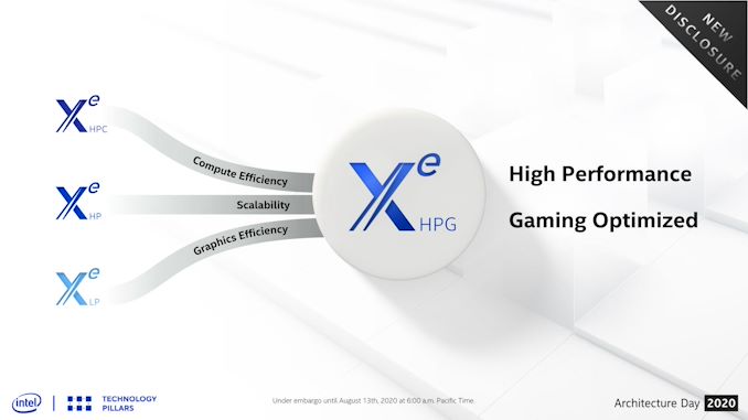
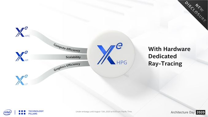
| 9:40a | Intel’s Xe-HPG GPU Unveiled: Built for Enthusiast Gamers, Built at a Third-Party Fab
Among the many announcements in today’s Intel Architecture Day, Intel is also offering a major update to their GPU roadmap over the next 24 months. The Xe family, already jam-packed with Xe-LP, Xe-HP, and Xe-HPC parts, is now getting a fourth planned variant: Xe-HPG. Aimed directly at the enthusiast gamer market, this latest Xe variant will be Intel’s most gaming-focused part yet, and the biggest step yet in Intel’s plans to be more diversified in its foundry sources. So what is Xe-HPG? At a high level, it’s meant to be the missing piece of the puzzle in Intel’s product stack, offering a high-performance gaming and graphics-focused chip. This is as opposed to Xe-HP, which is specializing in datacenter features like FP64 and multi-tile scalability, and Xe-HPC which is even more esoteric. In that respect, Xe-HPG can be thought of as everything in the Xe family, distilled down into a single design to push FLOPs, rays, pixels, and everything else a powerful video card might need.
Like with the rest of Intel’s forward-looking Xe announcements, the company isn’t offering performance projections, features, or the like. But we do have some small details on what to expect. First and foremost, beyond going after the enthusiast performance space, Intel has confirmed that this part will support ray tracing. A marquee feature of high-end video cards, ray tracing will take on even greater important over the coming years as the soon-to-launch next-generation consoles head out the door with the feature as well, eventually transforming it into a baseline feature across all gaming platforms. Similarly, ray tracing is a critical component of Microsoft’s DirectX 12 Ultimate standard, which given the timing of this GPU and Intel’s intentions, I would be shocked if Intel didn’t support in full.
The chip will be built on the foundation that is Xe-LP. However it will also pull in technologies that Intel is pioneering for Xe-HP, and Xe-HPC. Not the least of which is raw scalability, which is being able to take the Xe-LP foundation and scale it up to hundreds (if not thousands) of GPU execution units. But Intel is also pulling what they are calling “compute frequency enhancements” from Xe-HPC, which presumably will allow them to maximize the chip’s overall clockspeeds. All told, I won’t be too surprised if it looks a lot like Xe-HP in general, except with server-driven features like fast FP64 support and multi-tiling stripped out. But Xe-HPG will also bring something new to the table for the entire Xe family: GDDR6 support. Intel is confirming that the chip – or rather, the microarchitecture the chip will be based on – will be designed to work with GDRR6. This is as opposed to Xe-HP(C), which as high-end server parts use HBM, and Xe-LP, which is designed for use with more conventional memory types. GDDR6 compatibility is a unique need that reflects this is a gaming focused part: GDDR6 provides the memory bandwidth needed for high-performance graphics, but without the stratospheric costs of HBM memory (a problem that has impacted some other high-end GPUs over the years). In a further twist, Intel apparently licensed the GDDR controller IP from outside the company, rather than developing it in-house; so Xe-HPG will have a very notable bit of external IP in it.
But perhaps most interesting of all for graphics insiders and Intel investors alike is where Xe-HPG will be built: not at Intel. As part of their Architecture Day roadmap, Intel has confirmed that the part will be made at an external fab. In fact it’s the only Xe part where the GPU (or at least the compute element) is being made entirely at a third-party fab. Intel of course will not reveal which fab this is – if it’s TSMC or Samsung – but it means we’re going to see a complete Intel GPU built at another fab. If nothing else, this is going to make comparing Xe-HPG to its AMD and NVIDIA rivals a lot easier, since Intel will be using the same fab resources. Looking at the same roadmap, it’s worth pointing out that Intel won’t be using any of their advanced packaging technologies for the part. Since they’re not using HBM and they’re not doing multi-tiling, there’s no need for things like EMIB, never mind Foveros. There’s still a lot of unknowns with the cost aspects of Intel’s advanced packaging technologies, so keeping it out of Xe-HPG will presumably help keep costs in check in a very competitive marketplace. And that is the scoop on Xe-HPG. The latest and most gaming-focused member of Intel’s Xe GPU product stack is set to launch in 2021 – and as Intel looks to break into the wider GPU market, I don’t doubt for a second that this won’t be the last we’ll hear of it between then and now. |
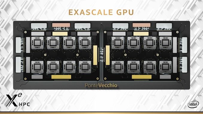
| 12:00p | Intel Xe-HPC GPU Status Update: 4 Process Nodes Make 1 Accelerator
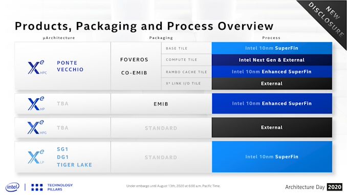
Continuing today’s GPU news from Intel’s Architecture Day presentation, on top of the Xe-LP architecture briefing and Xe-HPG reveal, the company has also offered a brief roadmap update for their flagship sever-level part, Xe-HPC. Better known by its codename of Ponte Vecchio, much to do has been made about Xe-HPC. The most complex of the Xe parts planned, it is also the cornerstone of the Intel-powered Aurora supercomputer. Xe-HPC is pulling out all of the stops for performance, and to get there Intel is employing every trick in the book, including their new-generation advanced packaging technologies.
The big revelation here is that we finally have some more concrete insight into what manufacturing processes the various tiles will use. The base tile of the GPU will be on Intel’s new 10nm SuperFin process, and the Rambo Cache will be a generation newer still, using Intel’s future 10nm Enhanced SuperFin process. Meanwhile it’s now confirmed that the Xe Link I/O tile, which will be used as part of Intel’s fabric to link together multiple Xe-HPC GPUs, will be built by an external fab. That leaves the matter of the compute tile, the most performance-critical of the GPU’s parts. With Intel’s 7nm process delayed by at least six months, the company has previously disclosed that they were going to take a “pragmatic” approach and potentially use third-party fabs. And as of their Architecture Day update, they still seem to be undecided about – or at least unwilling to disclose – just what they plan on doing. Instead, the compute die is labeled as “Intel Next Gen & External”. It's an unusual disclosure, to say the least, as we'd otherwise expect the compute die to be made on a single process. But with no further commentary from Intel offered, make of that what you will. Perhaps they’re being straightforward, and they will actually use two very different process nodes for the compute die? |


| << Previous Day |
2020/08/13 [Calendar] |
Next Day >> |