[Most Recent Entries] [Calendar View]
Friday, August 21st, 2020
- Intel Initiates EOL for the VCA2: Three Xeons on a PCIe Card
- Intel Announces Xeon E3-1500 v5: Iris Pro and eDRAM for Streaming Video
- The Intel Xe-LP GPU Architecture Deep Dive: Building Up The Next Generation
- Seeing Is Believing: Intel Teases DG1 Discrete Xe GPU With Laptop & Desktop Dev Cards At CES 2020
- Raja Koduri at Intel HPC Devcon Keynote Live Blog (4pm MT, 11pm UTC)
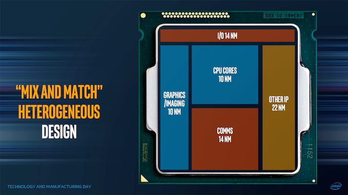
- The Intel Lakefield Deep Dive: Everything To Know About the First x86 Hybrid CPU
- Intel Next-Gen 10-micron Stacking: Going 3D Beyond Foveros
- An Interconnected Interview with Intel’s Ramune Nagisetty: A Future with Foveros
- Intel’s Xe for HPC: Ponte Vecchio with Chiplets, EMIB, and Foveros on 7nm, Coming 2021
- Intel’s EMIB Now Between Two High TDP Die: The New Stratix 10 GX 10M FPGA
- Intel's Interconnected Future: Combining Chiplets, EMIB, and Foveros
- Intel Launches Stratix 10 TX: Leveraging EMIB with 58G Transceivers
- Hot Chips 2020 Live Blog: Intel 10nm Agilex FPGAs (8:30am PT)
- Intel’s EMIB Now Between Two High TDP Die: The New Stratix 10 GX 10M FPGA
- Xilinx Announces World Largest FPGA: Virtex Ultrascale+ VU19P with 9m Cells
- Intel Agilex: 10nm FPGAs with PCIe 5.0, DDR5, and CXL
| Time | Event |
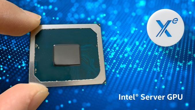
| 9:00a | Intel’s SG1 is 4x DG1: Xe-LP Graphics for Server Video Acceleration and Streaming
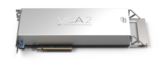
For the last few years, Intel has had a product line known as the Visual Computing Accelerator (VCA). With the VCA2 product being put on EOL earlier this year, without a replacement, we wondered where this market of Intel’s was going to go. At Intel’s Architecture Day 2020, it would appear the company is set to product a new SG1 graphics card for the server market for this purpose. Intel’s Visual Compute AcceleratorTwo versions of the VCA have existed, and the hardware underneath was relatively unorthodox – Intel put three of its Xeon E3 processors onto a single PCB behind a PCIe switch.
Each processor connected to its own DRAM and chipset as well, and the goal was to use the Intel Gen graphics on-board to be able to accelerate streaming video either for consumption or gaming. These processors had the best version of Intel’s Iris Pro P6300/P580 GT4e graphics, along with 128 MB of L4 eDRAM and 32 GB of DRAM each – we saw a company that built VCE cards for Intel’s partners back at Supercomputing 2019.
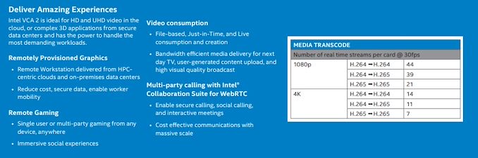
Each VCA2 was capable of transcoding 44 streams of 1080p30 H.264 simultaneously, or 14 streams of 4K30 H.264. However, the second generation VCA2 was put on the EOL path earlier this year, with no replacement in sight.
DG1 and SG1Intel declared during Architecture Day that it is planning three products built on its new Xe-LP graphics architecture. The company went into some detail about the form of Xe-LP graphics that will be going into the new Tiger Lake notebook processor, which will be the first version on the market (the full announcement of Tiger Lake is expected to be on September 2nd).
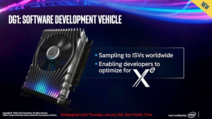
The other product previously announced on Xe-LP was DG1: Discrete Graphics 1. This is expected to be the first discrete PCIe add-in card for LP, targeting at the low-end market. Intel has already shown the software development vehicle for DG1 at CES in January 2020, with the announcement that they were starting to sample a version of the card to its software partners in advance of a bigger launch later in the year. The card was the same size of the low-to-mid range graphics on the market today, without a PCIe connector, indicating that it should be under 75W.
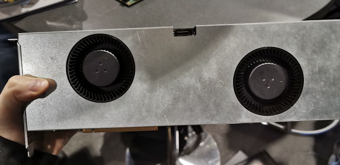
The third product is SG1: Server Graphics. Intel gave near zero details as to the setup of SG1, however they did mention that the target market was for video acceleration and streaming, exactly where the VCA series has sat. This would make it align with the mothballing of the current VCA series later this year. The VCA2 card was a GPU that had an 8-pin and a 6-pin power connector and 3x 45W CPUs as well as dual Ethernet outputs, so we fully expect SG1 to be of a similar size. Intel confirmed to us that SG1 will be a product containing four DG1 silicon dies, put on the same PCB. We expect there to be additional direct external networking connectivity and memory support, and it will be interesting to see how the PCIe lanes are distributed and configuration will be. Intel has confirmed that the new GPU supports AVC, HEVC, MPEG2, VP9 encode/decode and AV1 decode. Related Reading |
| 11:00a | Intel Xe-HP Graphics: Early Samples Offer 42+ TFLOPs of FP32 Performance
One of the promises that Intel has made with its new Xe GPU family is that in its various forms it will cater to uses ranging from integrated graphics all the way up to the high performance compute models needed for super-dense supercomputers. This means support for the types of calculations involved in simple graphics, complex graphics, ray tracing, AI inference, AI training, and the compute that goes into molecular modelling, oil-and-gas, nuclear reactors, rockets, nuclear rockets, and all the other big questions where more compute offers more capabilities. Sitting near the top of Intel’s offerings is the Xe-HP architecture, designed to offer high performance GPUs for standard server and enterprise deployments. |
| 12:00p | Cerebras Wafer Scale Engine News: DoE Supercomputer Gets 400,000 AI Cores
One of the more interesting AI silicon projects over the last couple of years has been the Cerebras Wafer Scale Engine, most notably for the fact that a single chip is the size of a literal wafer. Cerebras packs the WSE1 chip into a 15U custom liquid cooled server, called the CS-1, with a number of innovations regarding packaging, power, and setup. A single CS-1 requires about 20 kW of power peak, and costs around a couple million dollars (the Pittsburgh Supercomputing Center purchased two last year based on a $5m research grant). Cerebras say they have double digit customers and several dozen units already in the field, however today marks a considerable milestone as the US Department of Energy now has one deployed and working, attached directly to a supercomputer. |
| 1:00p | Intel’s Future 7nm FPGAs To Use Foveros 3D Stacking
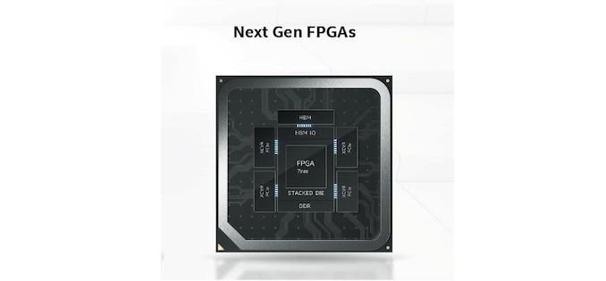
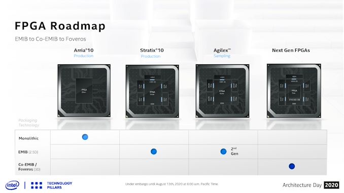
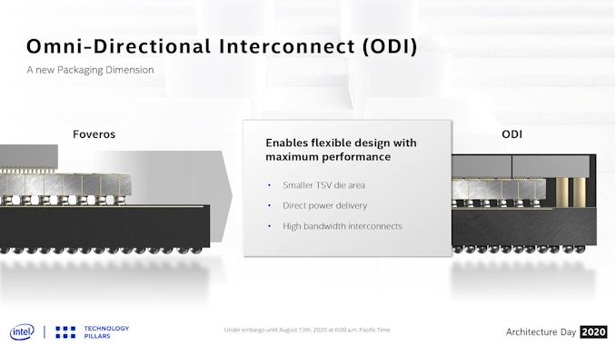
One of the main battlegrounds of future leading-edge semiconductor products will be in the packaging technology: being able to integrate multiple elements of silicon onto the same package with high bandwidth and low power interconnects will be, according to Intel, one way of extending the performance aspects of Moore’s Law into the next decade. Intel has three new parts to its advanced packaging portfolio: EMIB, Foveros, and ODI. At Intel’s Architecture Day 2020, we learned that Intel’s next generation of FPGA products, built on Intel’s own future 7nm manufacturing process, will integrate EMIB from its current generation as well as Foveros 3D stacking. EMIB, or Embedded Multi-Die Interconnect Bridge, is essentially a bit of silicon embedded into a PCB substrate that allows a silicon die to connect to it in a very dense way. Two bits of silicon can connect to a single EMIB, allowing a fast and low power point-to-point interconnect. We have seen EMIB in use with Kaby Lake-G, the Stratix 10 GX 10M FPGAs, and for upcoming variations of Intel’s Xe graphics portfolio, such as Ponte Vecchio and Xe-HP. Intel has also released a royalty free version of EMIB, called AIB, which has its own generation-on-generation upgrade path for use in the wider industry. Foveros is Intel’s die-to-die ‘3D’ stacking technology that allows two bits of silicon to connect on top of each other, again in a high-bandwidth and low power implementation. Foveros is currently in use in Intel’s Lakefield mobile processor, and has been announced for future products such as Ponte Vecchio. We now have another one to add to that list: FPGAs.
There is no distinct detail about what the next generation FPGAs would have, aside from Intel’s 7nm process and be stacked upon a base die that contains the HBM IO and DDR connections. I assume that the goal here is to have a common base die for a number of FPGA sizes, and then different variants of the 7nm FPGA could be stacked on top based on customer needs, or based on productization perhaps due to yield or cost or such. Technically Intel calls any product with both EMIB and Foveros a ‘Co-EMIB’ product, and this falls under that naming. One of the new elements that the 7nm FPGAs will have access to is a new 224G PAM4 transceiver module, which Intel is currently in the process of tuning and validating. It is unclear exactly when these new 7nm FPGAs will be launched – Intel’s own slide decks show a roadmap where the current 10nm Agilex FPGAs are the main products for 2021/2022, so we are perhaps looking at 2023 or later for these designs. They are far enough out that Intel doesn’t have it on the following roadmap:
A word on ODI, or Omni-Directional Interconnect. When a chip is built with Foveros, the high-power compute chip often has to be on top for thermal reasons, but the power for that compute chip has to travel through the base chip to reach the compute one. It also means that the top chips are smaller than the ones underneath. ODI solves this issue, by allowing the top chip to ‘hang’ over the edge, in a cantilevered fashion, such that the power connections from the base substrate can rise up through directly to the compute die. If there are enough power connections, then these connections can also be high-bandwidth data connections. This has added benefits in signal integrity, but also added complications in manufacturing and layout.
We expect ODI to be used more in the small-die space first, perhaps in future generations of ‘Lakefield’ type designs, rather than in FPGAs. Related Reading: |
| 3:00p | Intel’s New 224G PAM4 Transceivers
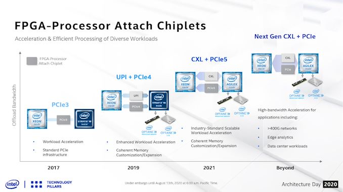
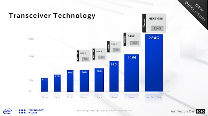
One battleground in the world of FPGAs is the transceiver – the ability to bring in (or push out) high speed signals onto an FPGA at low power. In a world where FPGAs offer the ultimate ability in re-programmable logic, having multiple transceivers to bring in the bandwidth is a key part of design. This is why SmartNICs and dense server-to-server interconnect topologies all rely on FPGAs for initial deployment and adaptation, before perhaps moving to an ASIC. As a result, the key FPGA companies that play in this space often look at high-speed transceiver adoption and design as part of the product portfolio.
In recent memory, Xilinx and Altera (now Intel), have been going back and forth, talking about 26G transceivers, 28G transceivers, 56G/58G, and we were given a glimpse into the 116G transceivers that Intel will implement as an option for its M-Series 10nm Agilex FPGAs back at Arch Day 2018. The Ethernet based 116G ‘F-Tile’ is a separate chiplet module connected to the central Agilex FPGA through an Embedded Multi-Die Interconnect Bridge (EMIB), as it is built on a different process to the main FPGA.
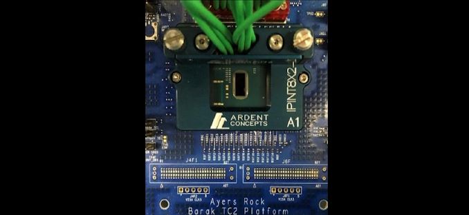
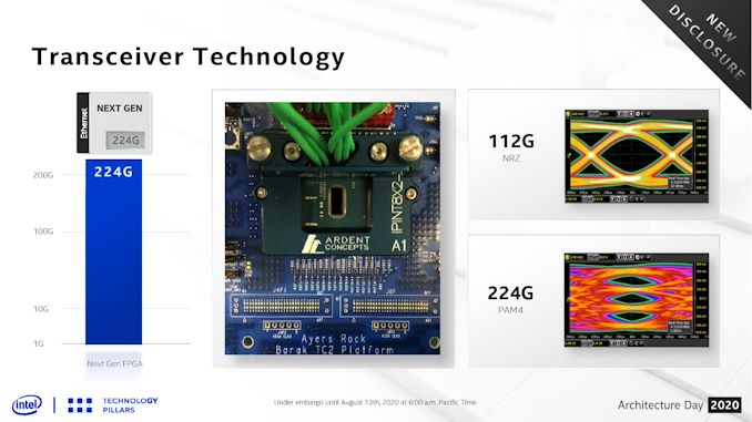
As part of Intel’s Architecture Day 2020, the company announced that it is now working on a new higher speed module, rated at 224G. This module is set to support both 224G in a PAM4 mode (4-bits) and 112G in an NRZ mode (2-bits). This should enable future generations of the Ethernet protocol stack, and Intel says it will be ready in late 2021/2022 and will be backwards compatible with the Agilex hardened 100/200/400 GbE stack. Intel didn’t go into any detail about bit-error rates or power at this time, but did show a couple of fancy eye diagrams. Related ReadingGallery: Intel’s New 224G PAM4 Transceivers
 _carousel_thumb.jpg) _carousel_thumb.jpg) |
| 3:30p | ASRock B550 Taichi Review: The $300 B550 Motherboard with Chutzpah Outside of its Aqua series of motherboards, which come with exquisitely crafted monoblocks, ASRock's Taichi brand has been a critical part of the company's offerings in the land of premium motherboards. The ASRock B550 Taichi sits at the top of its product stack and features an impressive quality feature set. Some of the most notable features include a large 16-phase power delivery, eight SATA ports, dual M.2 slots, an Intel 2.5 GbE Ethernet controller, and an Intel Wi-Fi 6 interface. At $300 it comes equal in price with the X570 version, which leaves questions on the table as to which one is actually worth the money. |
| 5:00p | Intel Moving to Chiplets: ‘Client 2.0’ for 7nm
One of the more esoteric elements of Intel’s Architecture Day 2020 came very near the end, where Intel spent a few minutes discussing what it believes is the future of some of its products. Brijesh Tripathi, VP and CTO of Intel’s Client Computing group, laid out a vision about the future of its client products in the 2024+ future timeframe. Centered around Intel’s 7+ manufacturing process, the goal was to enable ‘Client 2.0’ – a new way to deliver and enable immersive experiences through a more optimized silicon development strategy. |
_575px.jpg)


| << Previous Day |
2020/08/21 [Calendar] |
Next Day >> |