[Most Recent Entries] [Calendar View]
Friday, April 2nd, 2021
- First up, the company needs to build and equip its N5-capable fab in Arizona. The facility will cost around $12 billion, will have a capacity of 20,000 wafer starts per month (WSPM), and will come online in 2024. A recent rumor indicates that TSMC might actually increase capacity of the facility and/or equip it for a more advanced fabrication process, which will increase its cost, but TSMC has never confirmed this information.
- Secondly, TSMC will need to equip its N3-capable fab in Tainan, Taiwan, which is projected to start volume production in the second half of 2022.
- TSMC's third capital-expensive project is the company's N2 (2nm) qualified GigaFab in Hsinchu, Taiwan. Furthermore, TSMC is mulling to build another N2-capable fab in Baoshan, Taiwan. Meanwhile, TSMC still has to complete development of its GAAFET-based N2 node.
- Last but not least, TSMC is set to build two more advanced packaging facilities in Taiwan. The company already has four of such facilities, but it believes that demand for chip stacking and advanced packaging will rise in the future and it will need more capacities. Chip packaging factories are not as expensive as semiconductor production facilities, but they still cost quite a lot.
| Time | Event |
| 10:00a | TSMC to Spend $100B on Fabs and R&D Over Next Three Years: 2nm, Arizona Fab & More
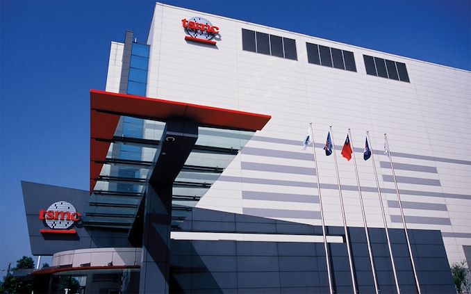
TSMC this week has announced plans to spend $100 billion on new production facilities as well as R&D over the next three years. The world's largest contract maker of chips says that its fabs are currently working at full load, so to meet demand for its services going forward it will need (much) more capacity. Among TSMC's facilities to go online in the next three to four years are the company's fab in Arizona as well as its first 2nm-capable fab in Taiwan. "TSMC is entering a period of higher growth as the multiyear megatrends of 5G and HPC are expected to fuel strong demand for our semiconductor technologies in the next several years," a statement by TSMC with the Taiwan Stock Exchange reads. "In addition, the COVID-19 pandemic also accelerates digitalization in every aspect. In order to keep up with demand, TSMC expects to invest $100 billion over the next three years to increase capacity to support the manufacturing and R&D of advanced semiconductor technologies. TSMC is working closely with our customers to address their needs in a sustainable manner." $100 Billion to Be Spent on FabsTSMC's capital expenditures (CapEx) budget last year was $17.2 billion, whereas its R&D budget was $3.72 billion, or approximately 8.2% of its revenue. This year the company intends to increase its CapEx to somewhere in the range of $25 to $28 billion, which would make for a 45% to 62% year-over-year increase in that spending. The company's R&D spending will also rise as its revenue is expected to grow. In total, TSMC plans to invest around $30 billion or more on CapEx and R&D this year. Taken altogether, if the company intends to spend around $100 billion from 2021 through 2023, its expenditures in the next two years will be roughly flat with 2021, something that should please its investors. TSMC has a number of important fab projects ahead of it. Recently TSMC wrote a letter to its customers where it explained that its fabs have been fully utilized for about a year now and it still cannot meet rising demand for chips. To that end, the company would have to 'suspend wafer price reductions for a year from the start of 2022,' according to a Bloomberg report. Competition IntensifyingRight now, TSMC is the world's largest contract maker of chips with no rivals that can match its total production capacity. A some of TSMC's rivals, including GlobalFoundries and UMC, have pulled the plug on development of their leading-edge fabrication processes, so the number of companies that can offer leading-edge nodes has decreased. Yet paradoxically, the competition is also escalating in other respects. Samsung Semiconductor, which has foundry, DRAM, storage, SoC, and a number of other operations, has been increasing its CapEx investments in the recent years. The company spent $93.2 billion on chip production from 2017 to 2020 and is on track spend another ~$28 billion in 2021, according to IC Insights. Samsung Foundry is still several times smaller than TSMC in terms of sales and capacity, but the gap is closing. In addition to Samsung Foundry, Intel recently introduced its integrated device manufacturer 2.0 (IDM 2.0) plan that includes offering advanced foundry services and essentially compete against TSMC (while also using its services when needed). Intel has already announced plans to invest $20 billion in two new fabs in Arizona and said it would invest more in expansion of chip production in other parts of the USA as well as in Europe and other parts of the world. To stay ahead of existing and emerging rivals, TSMC needs to keep investing in R&D and expand its production capacities, so a $100 billion investment plan will be instrumental for these purposes. |
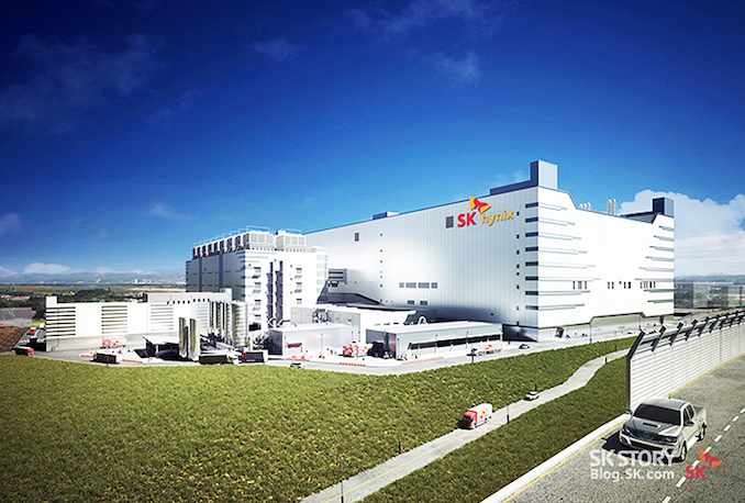
| 1:00p | SK Hynix to Build $106 Billion Fab Cluster: 800,000 Wafer Starts a Month
Capping off a busy week for fab-related news, South Korea authorities this week gave SK Hynix a green light to build a new, 120 trillion won ($106.35 billion) fab complex. The fab cluster will be primarily used to build DRAM for PCs, mobile devices, and servers, using process technologies that rely on extreme ultraviolet lithography (EUV). The first fab in the complex will go online in 2025. The new cluster will house four huge semiconductor fabrication plants, which will be located on a 4.15 million square-meter site, reports The Korea Herald. The four fabs will have a planned capacity of around 800,000 wafer starts per month (WSPM), which will make the site one of the world's biggest semiconductor production hubs. Keeping in mind that we are dealing with EUV fabs, it is not surprising that a huge 200,000-WSPM plant with EUV tools will cost SK Hynix north of $25 billion. The fab cluster will be located near Yongin, South Korea, 50 kilometers south of Seoul, according to Yonhap news agency that cites the Ministry of Trade, Industry and Energy. The new fabs will be used to make various types of DRAM using SK Hynix's upcoming production technologies that will use extreme ultraviolet (EUV) lithography. And with a start date still years away, we're likely looking at a fab that will be used to manufacture DDR5, LPDDR5X, and other future types of DRAM. SK Hynix reportedly plans to start construction of the first fab in the Yongin cluster in the fourth quarter of 2021. Given the expected size of the massive building and the amount of time needed to folly load it with production equipment, SK Hynix expects this first fab to be completed in 2025. It is necessary to note that just several years ago SK Hynix and Samsung used to build fabs that could produce both DRAM and NAND flash memory – or at least be converted with a minimal amount of effort. This is not the case today as DRAM production now heavily relies on lithography equipment, whereas 3D NAND production uses loads of etching tools, which is why the fabs for different types of memory have to be equipped completely differently. The fab cluster in Yongin will be SK Hynix's second major DRAM site in South Korea after the company's primary DRAM hub near Icheon that houses its M10, M14, and M16 fabs. The M16 fab was completed in February and will be used for DRAM production using SK Hynix's EUV-based 1a process technology starting the second half of 2021. |
| << Previous Day |
2021/04/02 [Calendar] |
Next Day >> |