[Most Recent Entries] [Calendar View]
Thursday, November 18th, 2021
| Time | Event |
| 6:00a | Sponsored Post: Supermicro Discussed the Future of HPC at SC 21
Supermicro took an in-depth look at everything from modular GPUs, to liquid cooling. Check out what you missed. |
| 8:00a | AMD’s Instinct MI250X: Ready For Deployment at Supercomputing
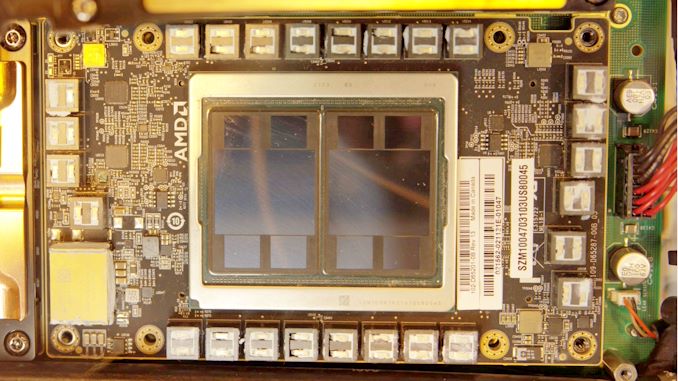
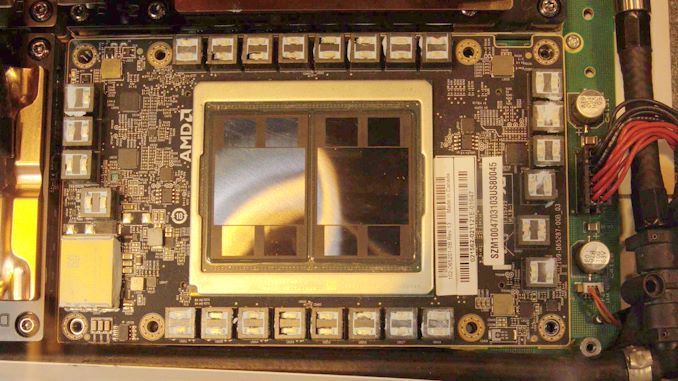
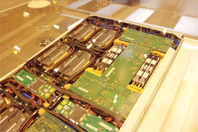
One of the big announcements at AMD’s Data Center event a couple of weeks ago was the announcement of its CDNA2 based compute accelerator, the Instinct MI250X. The MI250X uses two MI200 Graphics Compute Dies on TSMC’s N6 manufacturing node, along with four HBM2E modules per die, using a new ‘2.5D’ packaging design that uses a bridge between the die and the substrate for high performance and low power connectivity. This is the GPU going into Frontier, one of the US Exascale systems due for power on very shortly. At the Supercomputing conference this week, HPE, under the HPE Cray brand, had one of those blades on display, along with a full frontal die shot of the MI250X. Many thanks to Patrick Kennedy from ServeTheHome for sharing these images and giving us permission to republish them.
The MI250X chip is a shimmed package in an OAM form factor. OAM stands for OCP Accelerator Module, which was developed by the Open Compute Project (OCP) – an industry standards body for servers and performance computing. And this is the accelerator form factor standard the partners use, especially when you pack a lot of these into a system. Eight of them, to be exact.
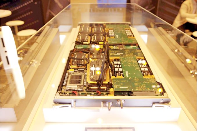
This is a 1U half-blade, featuring two nodes. Each node is an AMD EPYC ‘Trento’ CPU (that’s a custom IO version of Milan using the Infinity Fabric) paired with four MI250X accelerators. Everything is liquid cooled. AMD said that the MI250X can go up to 560 W per accelerator, so eight of those plus two CPUs could mean this unit requires 5 kilowatts of power and cooling. If this is only a half-blade, then we’re talking some serious compute and power density here.
Each node seems relatively self-contained – the CPU on the right here isn’t upside down given the socket rear pin outs aren’t visible, but that’s liquid cooled as well. What looks like four copper heatpipes, two on each side of the CPU, is actually a full 8-channel memory configuration. These servers don’t have power supplies, but they get the power from a unified back-plane in the rack.
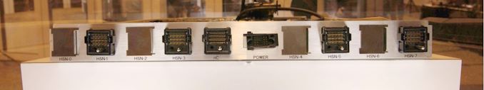
The back connectors look something like this. Each rack of Frontier nodes will be using HPE’s Slingshot interconnect fabric to scale out across the whole supercomputer.
Systems like this are undoubtedly over-engineered for the sake of sustained reliability – that’s why we have as much cooling as you can get, enough power phases for a 560 W accelerator, and even with this image, you can see those base motherboards the OAM connects into are easily 16 layers, if not 20 or 24. For reference, a budget consumer motherboard today might only have four layers, while enthusiast motherboards have 8 or 10, sometimes 12 for HEDT. In the global press briefing, Keynote Chair and Professor world renowned HPC Professor Jack Dongarra, suggested that Frontier is very close to being powered up to be one of the first exascale systems in the US. He didn’t outright say it would beat the Aurora supercomputer (Sapphire Rapids + Ponte Vecchio) to the title of first, as he doesn’t have the same insight into that system, but he sounded hopeful that Frontier would submit a 1+ ExaFLOP score to the TOP500 list in June 2021. Many thanks to Patrick Kennedy and ServeTheHome for permission to share his images. |
| 12:15p | Qualcomm x Nuvia: Silicon Sampling in Late 2022, Products in 2023
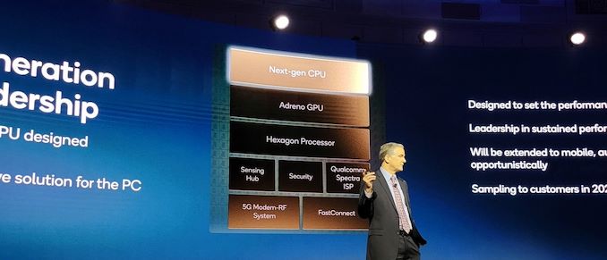
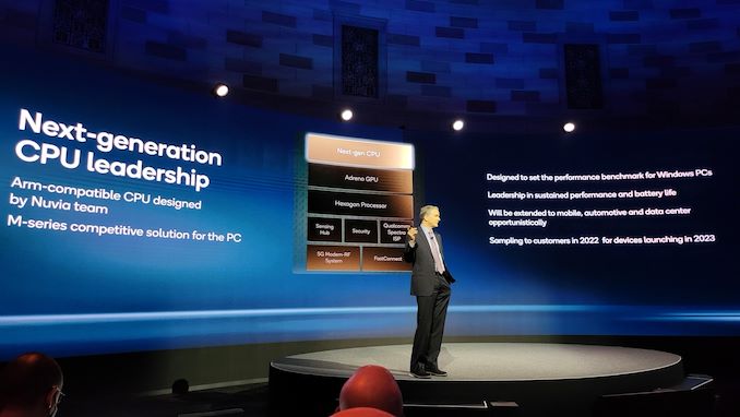
One of the more curious acquisitions in the last couple of years has been that of Nuvia by Qualcomm. Nuvia was a Silicon Valley start-up founded by the key silicon and design engineers and architects behind both Apple’s and Google’s silicon for the past few years. Qualcomm CEO Cristiano Amon made it crystal clear when Nuvia was acquired that they were going after the high-performance ultraportable laptop market, with both Intel and Apple in the crosshairs. Nuvia came out of stealth in November 2019, with the three main founders having spent almost a year building the company. Gerard Williams III, John Bruno, and Manu Gulati have collectively driven the silicon design of 20+ chips, have combined over 100 patent, and have been in leadership roles across Google, Apple, Arm, Broadcom, and AMD. Nuvia raised a lot of capital, $300M+ over two rounds of funding and angel investors, and the company hired a lot of impressive staff. The goal of Nuvia was to build an Arm-based general purpose server chip that would rock the industry. Imagine something similar to what Graviton 2 and Ampere Altra are today, but with a custom microarchitecture on par (or better) with Apple’s current designs. When Nuvia was still on its own in start-up mode, some were heralding the team and the prospect, calling for the downfall of x86 with Nuvia’s approach. However, Qualcomm swept in and acquired the company in March 2021, and repurposed Nuvia’s efforts towards a laptop processor. It’s been no secret that Qualcomm has been after the laptop and notebook market for some time. Multiple generations of ‘Windows on Snapdragon’ have come to market through Qualcomm’s partners, initially featuring smartphone-class silicon before becoming something more bespoke with the 8cx, 8cx Gen 2, and 7c/7 options in the past couple of years. It has taken several years for Qualcomm to get the silicon and the Windows ecosystem somewhere that makes sense for commercial and consumer use, and with the recent news that Windows 11 on these devices now enabling full x86-64 emulation support, the functional difference between a Qualcomm laptop and an x86 laptop is supposed to be near zero. Qualcomm would argue their proposition is better, allowing for 2 days of use on a single charge, holding charge for weeks, and mobile wireless connectivity with 4G/5G. I’ve tested one of the previous generation S855 Lenovo Yoga devices, and the battery life is insane – but I needed better were functional support (turns out I have an abnormal edge-case work flow…) and more performance. While Qualcomm has been working on the former since my last test, and Nuvia is set to bring the latter.
At Qualcomm’s Investor Day this week, the Qualcomm/Nuvia relationship was mentioned in an update. I had hoped that by the end of this year (and Qualcomm’s Tech Summit in only a couple of weeks) that we might be seeing something regarding details or performance, however Qualcomm is stating that its original schedule is still on track. As announced at the acquisition, the goal is to deliver test silicon into the hands of partners in the second half of 2022. The goal here is to have laptop silicon that is competitive with Apple's M-series, but running Windows. This means blowing past Intel and AMD offerings, and coupled with the benefits of better battery life, sustained performance, and mobile connectivity. From the disclosures so far, it’s perhaps no surprise that the Nuvia CPUs will be paired with an Adreno GPU and a Hexagon DSP, although it will be interesting to see if the Nuvia CPU is a single big core paired with regular Arm efficient cores, or everything in the CPU side will be new from the Nuvia team. I have no doubt that at Qualcomm’s Tech Summit in December 2022 we’ll get a deeper insight into the microarchitecture of the new core. Either that or Qualcomm might surprise us with a Hot Chips presentation in August. With regards to going beyond laptop chips, while Qualcomm is happy to state that Nuvia's designs will be 'extended to [other areas] opportunistically', it's clear that they're locking the crosshairs on the laptop market before even considering what else might be in the field of view. |
| 6:00p | MediaTek Announces Dimensity 9000: Supercharged Flagship SoC on 4nm Today, MediaTek is re-entering the flagship SoC space with a bang. The Dimensity 9000 is the first Armv9 SoC, with X2, A710 and A510 cores, large new GPU, massive new ISP, first LPDDR5X, and all in a new TSMC N4 process node. |


| << Previous Day |
2021/11/18 [Calendar] |
Next Day >> |