[Most Recent Entries] [Calendar View]
Friday, July 12th, 2024
| Time | Event |
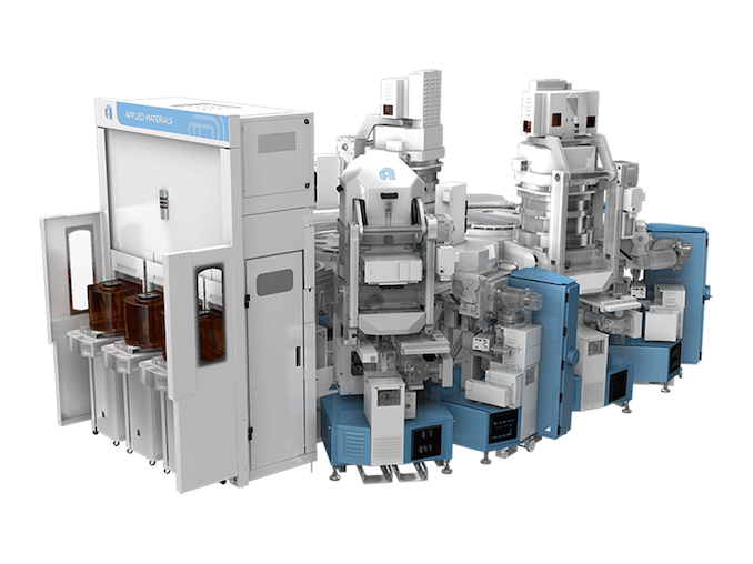
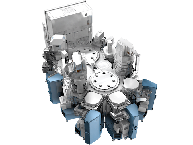
| 8:00a | Applied Materials' New Deposition Tool Enables Copper Wires to Be Used for 2nm and Beyond
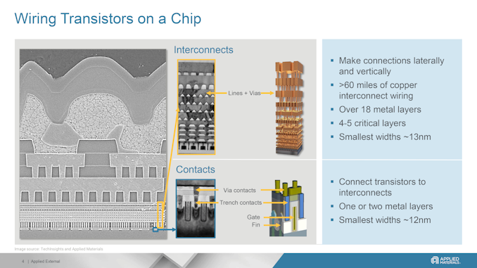
Although the pace of Moore's Law has undeniably slackened in the last decade, transistor density is still increasing with every new process technology. But there is a challenge with feeding power to smaller transistors, as with the smaller transistors comes thinner power wires within the chip, which increases their resistance and may cause yield loss. Looking to combat that effect, this week Applied Materials introduced its new Applied Endura Copper Barrier Seed IMS with Volta Ruthenium Copper Vapor Deposition (CVD) tool, which enables chipmakers to keep using copper for wiring with 2 nm-class and more advanced process technologies. Today's advanced logic processors have about 20 layers of metal, with thin signal wires and thicker power wires. Scaling down wiring with shrinking transistors presents numerous challenges. Thinner wires have higher electrical resistance, while closer wires heighten capacitance and electrical crosstalk. The combination of the two can lead to increased power consumption while also limiting performance scaling, which is particularly problematic for datacenter grade processors that are looking to have it all. Moving power rails to a wafer's back-side is expected to enhance performance and efficiency by reducing wiring complexity and freeing up space for more transistors.
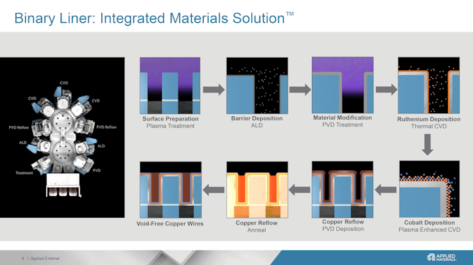
But backside power delivery network (BSPDN) does not solve the problem with thin wires in general. As lithographic scaling progresses, both transistor features and wiring trenches become smaller. This reduction means that barriers and liners take up more space in these trenches, leaving insufficient room to deposit copper without creating voids, which raises resistance and can lower yields. Additionally, the closer proximity of wires thins the low-k dielectrics, making them more vulnerable to damage during the etching process. This damage increases capacitance and weakens the chips, making them unsuitable for 3D stacking. Consequently, as the industry advances, copper wiring faces significant physical scaling challenges. But Applied Materials has a solution. Adopting Binary RuCo LinersContemporary manufacturing technologies use reflow to fill interconnects with copper, where anneals help the copper flow from the wafer surface into wiring trenches and vias. This process depends on the liners on which the copper flows. Normally, a CVD cobalt film was used for liners, but this film is too thick for 3nm-class nodes (which would affect resistance and yield).
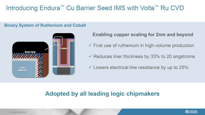
Applied Materials proposes using a ruthenium cobalt (RuCo) binary liner with a thickness under 20A (2nm, 20 angstroms), which would provide better surface properties for copper reflow. This would ultimately allow for 33% more space for void-free conductive copper to be reflowed, reducing the overall resistance by 25%. While usage of the new liner requires new tooling, it can enable better interconnects that mean higher performance, lower power consumption and higher yields.
Applied Materials says that so far its new Endura Copper Barrier Seed IMS with Volta Ruthenium CVD tool has been adopted by all leading logic makers, including TSMC and Samsung Foundry for their 3nm-class nodes and beyond.
"The semiconductor industry must deliver dramatic improvements in energy-efficient performance to enable sustainable growth in AI computing," said Dr. Y.J. Mii, Executive Vice President and Co-Chief Operating Officer at TSMC. "New materials that reduce interconnect resistance will play an important role in the semiconductor industry, alongside other innovations to improve overall system performance and power." New Low-K DielectricBut thin and efficient liner is not the only thing crucial for wiring at 3nm production nodes and beyond. Trenches for wiring are filed not only with a Co/RuCo liner and a Ta/N barrier, but with low dielectric constant (Low-K) film to minimize electrical charge buildup, reduce power consumption, and lower signal interference. Applied Materials has offered its Black Diamond Low-K film since the early 2000s. But new production nodes require better dielectrics, so this week the company introduced an upgraded version of Black Diamond material and a plasma-enhanced chemical vapor deposition (PEVCD) tool to apply it, the Producer Black Diamond PECVD series. This new material allows for scaling down to 2nm and beyond by further reducing the dielectric constant while also increasing the mechanical strength of the chips, which is good for 3D stacking both for logic and memory. The new Black Diamond is being rapidly adopted by major logic and DRAM chipmakers, Applied says. "The AI era needs more energy-efficient computing, and chip wiring and stacking are critical to performance and power consumption," said Dr. Prabu Raja, President of the Semiconductor Products Group at Applied Materials. "Applied's newest integrated materials solution enables the industry to scale low-resistance copper wiring to the emerging angstrom nodes, while our latest low-k dielectric material simultaneously reduces capacitance and strengthens chips to take 3D stacking to new heights."
|
| 4:30p | Troubled AI Processor Developer Graphcore Finds a Buyer: SoftBank
After months of searching for a buyer, troubled U.K.-based AI processor designer Graphcore said on Friday that it has been acquired by SoftBank. The company will operate as a wholly owned subsidiary of SoftBank and will possibly collaborate with Arm, but what remains to be seen what happens to the unique architecture of Graphcore's intelligence processing units (IPUs). Graphcore will retain its name as it will become a wholly owned subsidiary of SoftBank, which paid either $400 million (according to EE Times) or $500 million (according to BBC) for the company. Over its lifetime, Graphcore has received a total of $700 million of investments from Microsoft and Sequoia Capital, and at its peak in late 2020, was valued at $2.8 billion. Nigel Toon will remain at the helm of Graphcore, which will hire new staff in its UK offices and continue to be headquartered in Bristol, with additional offices in Cambridge, London, Gdansk (Poland), and Hsinchu (China). "This is a tremendous endorsement of our team and their ability to build truly transformative AI technologies at scale, as well as a great outcome for our company," said Nigel Toon. "Demand for AI compute is vast and continues to grow. There remains much to do to improve efficiency, resilience, and computational power to unlock the full potential of AI. In SoftBank, we have a partner that can enable the Graphcore team to redefine the landscape for AI technology."
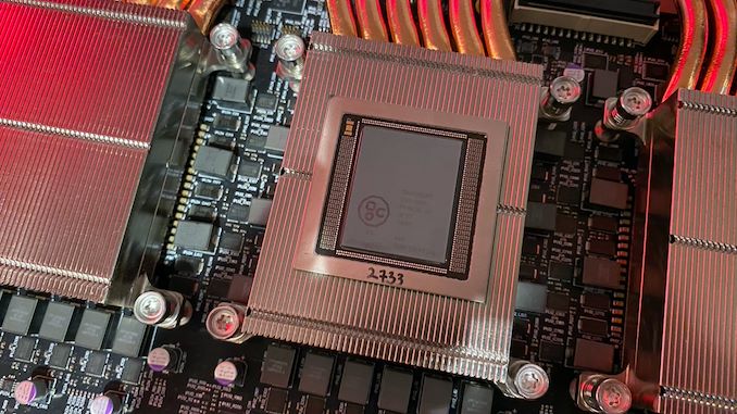
Although Graphcore says that it had won contracts with major high-tech companies and deployed its IPUs, it could not compete against NVIDIA and other prêt-à-porter AI processor vendors due to insufficient funding. In the recent years the company's problems were so severe that it had to lay off 20% of its staff, bringing its headcount to around 500. Those cuts also saw office closures in Norway, Japan, and South Korea, which made it even harder to compete against big players. Graphcore certainly hopes that with SoftBank's deep pockets and willingness to invest in AI technologies in general and AI processors in particular, it will finally be able to compete head-to-head with established players like NVIDIA. When asked whether Graphcore will work with SoftBank's Arm, Nigel Toon said that he was looking forward to work with all companies controlled by its parent, including Arm. Meanwhile, SoftBank itself is reportedly looking forward to build its own AI processor venture called Project Izanagi to compete against NVIDIA, whereas Arm is reportedly developing AI processors that will work in datacenters owned by SoftBank. Therefore, it remains to be seen where does Graphcore fit in. For now, the best processor that Graphcore has is its Colossus MK2 IPU, which is built using 59.4 billion transistors and packs in 1,472 independent cores with simultaneous multithreading (SMT) capable of handling 8,832 parallel threads. Instead of using HBM or other types of external memory, the chip integrates 900 MB of SRAM, providing an aggregated bandwidth of 47.5 TB/s per chip. Additionally, it features 10 IPU links to scale with other MK2 processors. When it comes to performance, the MK2 C600 delivers 560 TFLOPS FP8, 280 TFLOPS FP16, and 70 TFLOPS of FP32 performance at 185W. To put the numbers into context, NVIDIA's A100 delivers 312 FP16 TFLOPS without sparsity as well as 19.5 FP32 TFLOPS, whereas NVIDIA's H100 card offers 3,341 FP8 TFLOPS. |


| << Previous Day |
2024/07/12 [Calendar] |
Next Day >> |