[Most Recent Entries] [Calendar View]
Wednesday, March 4th, 2020
- Sizing Up The 5G Modem Market: Qualcomm, Intel, Huawei, Samsung, UniSOC, and Mediatek
- CES 2020: MediaTek Announces New Dimensity 800 Mid-Range 5G SoC
- Qualcomm Announces Snapdragon 865 and 765(G): 5G For All in 2020, All The Details
- Qualcomm’s New 3rd Generation Snapdragon X60 5G Modem, Built on 5nm
- Phanteks Unveils AMP: Inexpensive Modular PSUs up to 750W
- EVGA Enters SFX Market with SuperNOVA GM SFX PSUs
- Going BIG: EVGA’s SuperNova 2000W G+ Power Supply
- The SilverStone Strider Platinum ST1200-PTS 1200W PSU Review: Small in Size, Big on Compliance
- SilverStone’s 1000W SFX-L PSU: When Less Is More
- Arm & TSMC Showcase 7nm Chiplet, Eight A72 at 4GHz on CoWoS Interposer
- TSMC Boosts CapEx by $1 Billion, Expects N5 Node to Be Major Success
- Hot Chips 31 Keynote Day 2: Dr. Phillip Wong, VP Research at TSMC (1:45pm PT)
- TSMC Announces Performance-Enhanced 7nm & 5nm Process Technologies
- TSMC: First 7nm EUV Chips Taped Out, 5nm Risk Production in Q2 2019
- TSMC Kicks Off Volume Production of 7nm Chips
| Time | Event | |||||||||||||||||||||||||||||||||||||||||||||||||||||||||||||||||||||||||||||||||||||||||||||||||||||||||||||||||||||||||||
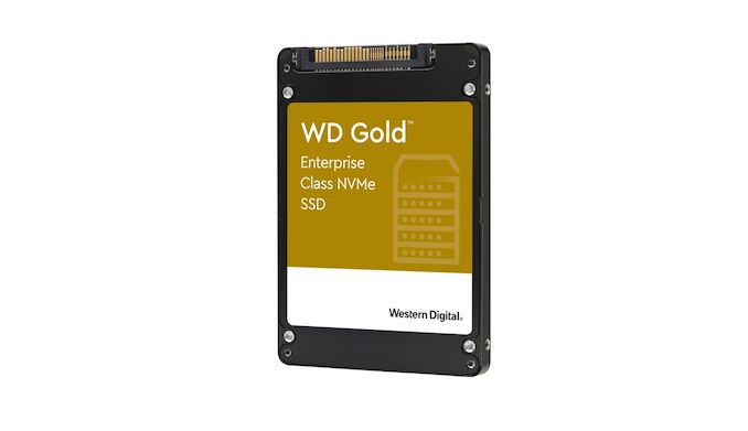
| 8:00a | Western Digital Introduces WD Gold Enterprise SSDs
On what would have been the first day of the Open Compute Project's annual Global Summit, Western Digital is bringing out a new line of enterprise SSDs. The WD Gold brand for enterprise drives is getting an SSD counterpart to the existing WD Gold enterprise hard drives. WD's color-based drive branding now features both SSDs and hard drives in almost every product segment: Blue and Green mainstream consumer drives, Black for high-end consumer, Red for NAS systems, and Gold for enterprise. The only one missing an SSD option is the WD Purple family for video surveillance recording (though there is a WD Purple microSD card). The new WD Gold SSD isn't anything new technologically; it's basically a re-branding of a portion of the Ultrastar DC SN640 product line. Where the WD Gold differs is in the target markets: Like other WD (color) products, the WD Gold SSD is intended for channel and retail sales rather than the large-scale direct B2B sales model used for Western Digital's Ultrastar datacenter drives and their client OEM drives. The WD Gold SSD will make Western Digital's enterprise SSD technology more accessible to small and medium enterprise customers.
The WD Gold SSD is based on the same hardware as the Ultrastar DC SN640 series, but the WD Gold product line doesn't include as many options. The SN640 comes in two endurance tiers: 0.8 drive writes per day and 2 DWPD. The WD Gold SSD line only includes the 0.8 DWPD drives, and only the U.2 form factor versions: a total of four capacity options from 960 GB up to 7.68 TB. These drives use the latest Western Digital/Kioxia 96-layer 3D TLC NAND flash memory and one of Western Digital's own in-house NVMe controller designs. The technical specs for the WD Gold SSDs are identical to the matching Ultrastar DC SN640 models. The performance is limited largely by the PCIe 3.0 interface and the power/thermal constraints of the 2.5"/7mm U.2 form factor: these drives idle just under 5W and can draw up to 12 W under load, with configurable power states to throttle down to 10 or 11 W for high-density deployments that can't quite keep them cool at the full 12W each. The WD Gold SSDs are planned to ship starting in early Q2. Pricing has not been announced. | |||||||||||||||||||||||||||||||||||||||||||||||||||||||||||||||||||||||||||||||||||||||||||||||||||||||||||||||||||||||||||
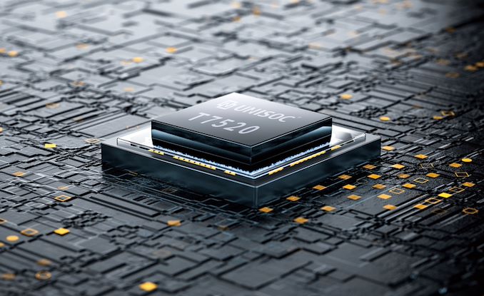
| 10:00a | UNISOC Unveils T7520 SoC for 5G Smartphones: Octa-Core, 6nm EUV
UNISOC, formerly Spreadtrum Semiconductor, has announced its first mobile application processor with an integrated 5G modem. Dubbed the T7520, the SoC also happens to be one of the world’s first chips to be made using TSMC’s 6 nm process technology, which uses extreme ultraviolet lithography (EUVL) for several layers. The UNISOC T7520 application processor packs four high-performance Arm Cortex-A76 cores, four energy-efficient Arm Cortex-A55 cores, as well as an Arm Mali-G57 GPU with a display engine that supports multiple screens with a 4K resolution and HDR10+. Furthermore, the SoC integrates a new NPU that is said to offer a 50% higher TOPS-per-Watt rate than the company’s previous-generation NPU. In addition, the chip features a four-core ISP that supports up to 100 MP sensors and multi-camera processing capability. Finally, the AP also features the company’s latest Secure Element processor that supports ‘most of crypto algorithms’ and can handle compute-intensive security scenarios, such as encrypted video calls. One of the key features of the UNISOC T7520 is of course its integrated 2G/3G/4G/5G-supporting modem, which supports 5G NR TDD+FDD carrier aggregation, as well as uplink and downlink decoupling for enhanced coverage. All told, the T7520's modem is designed to offer peak uplink speed of 3.25 Gbps. The high level of integration of the T7520 SoC is designed to enable smartphone manufacturers to build more reasonably priced 5G handsets, which will inevitably increase their popularity and adoption of the technology. Meanwhile, usage of TSMC’s 6 nm fabrication technology (known as N6) should allow UNISOC to make the AP for less than compared to non-EUV fabrication processes. UNISOC did not announce when it plans to start shipments of its T7520 application processor, though it is reasonable to expect it to become available this year. Related Reading: Source: UNISOC | |||||||||||||||||||||||||||||||||||||||||||||||||||||||||||||||||||||||||||||||||||||||||||||||||||||||||||||||||||||||||||
| 11:30a | Intel CFO: Our 10nm Will Be Less Profitable than 22nm [Morgan Stanley Transcription] This week at Morgan Stanley’s Analyst Conference, Intel’s CFO, George Davis, sat down to discuss the future of where Intel’s profitability lies. No stranger to the odd comments relating to how Intel manages its money, Mr. Davis was on fine form explaining that Intel is going to be in for a rough time as it corresponds to the leading edge. Among the statements made, Mr. Davis confirmed that Intel’s new 10nm node will be less profitable than its 22 nm node, let alone its 14 nm node. | |||||||||||||||||||||||||||||||||||||||||||||||||||||||||||||||||||||||||||||||||||||||||||||||||||||||||||||||||||||||||||
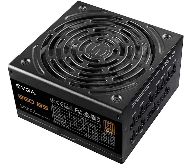
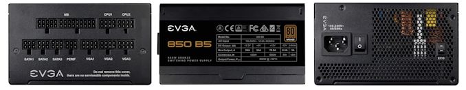
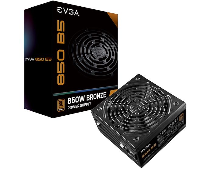
| 12:00p | EVGA Launches B5 Modular PSUs: 80Plus Bronze At Up to 850 W
EVGA this week has introduced a new family of entry-level, 80Plus power supplies. Promise to bring together strong performance, a rich feature set, and a relatively low price, EVGA’s modular B5-series PSUs are designed to tick all of the boxes expected for a basic PSU in 2020. The EVGA B5-series PSU family includes 550 W, 650 W, 750 W, and 850 W models, and are compliant with the latest ATX12 v2.52/EPS12V specifications. Fully modular, the most powerful SKU has six 8-pin PCIe power connectors, the 750 W model features four 8-pin PCIe power plugs, the 650 W flavor has three, whereas the entry 550 W model has two 8-pin PCIe power connectors. Obviously, the PSUs have SATA as well as Molex plugs too. The new power supplies correspond to the 80Plus Bronze requirements, so they are they are mandated to be 81% - 88% efficient under a 20% or 50% load as well as 81% - 85% efficient under a 100% load.
EVGA’s latest B5-series PSUs use 100% Japanese capacitors on 750 W and 850 W models (and some on less powerful SKUs), and feature an no-fan/ECO mode that shuts down the 135-mm fluid-dynamic bearing fan under low and medium loads. In addition, the power supplies feature a comprehensive set of protection technologies that includes OVP (Over Voltage Protection), UVP (Under Voltage Protection), OCP (Over Current Protection), OPP (Over Power Protection), SCP (Short Circuit Protection), and OTP (Over Temperature Protection).
EVGA’s B5-series power supplies measure 150x50x86 mm, which is pretty typical for mid-capacity PSUs, so they should easily fit into virtually any standard ATX case. And as mentioned earlier, the PSUs are fully modular, so they provide additional flexibility to system builders.
EVGA’s B5-series PSUs are immediately available directly from the company. The cheapest model, the 550 W version, is priced at $79.99, whereas the most powerful 850 W SKU is priced at $129.99. The power supplies are covered by a five-year warranty, which is typical for inexpensive PSUs.
Related Reading: Source: EVGA | |||||||||||||||||||||||||||||||||||||||||||||||||||||||||||||||||||||||||||||||||||||||||||||||||||||||||||||||||||||||||||
| 1:00p | El Capitan Supercomputer Detailed: AMD CPUs & GPUs To Drive 2 Exaflops of Compute Back in August, the United States Department of Energy and Cray announced plans for a third United States exascale supercomputer, El Capitan. Scheduled to be installed in Lawrence Livermore National Laboratory (LLNL) in early 2023, the system is intended primarily (but not exclusively) for use by the National Nuclear Security Administration (NNSA), who uses supercomputers in their ongoing nuclear weapons modeling. At the time the system was announced, The DOE and LLNL confirmed that they would be buying a Shasta system from Cray (now part of HPE), however the announcement at the time didn’t go into any detail about what hardware would actually be filling one of Cray’s very flexible supercomputers. But as of today, the wait is over. This afternoon the DOE and HPE are announcing the architectural details of the supercomputer, revealing that AMD will be providing both the CPUs and accelerators (GPUs), as well as revising the performance estimate for the supercomputer. Already expected to be the fastest of the US’s exascale systems, El Capitan was originally commissioned as a 1.5 exaflop system seven months ago. However thanks to some late configuration changes, the DOE now expects the system to reach 2 exaflops once it’s fully installed, which would cement its place at the top of the US’s supercomputer inventory. | |||||||||||||||||||||||||||||||||||||||||||||||||||||||||||||||||||||||||||||||||||||||||||||||||||||||||||||||||||||||||||
| 7:00p | TSMC & Broadcom Develop 1,700 mm2 CoWoS Interposer: 2X Larger Than Reticles
With transistor shrinks slowing and demand for HPC gear growing, as of late there has been an increased interest in chip solutions larger than the reticle size of a lithography machine – that is, chips bigger than the maximum size that a single chip can be produced. We've already seen efforts such as Cerebras' truly massive 1.2 trillion transistor wafer scale engine, and they aren't alone. As it turns out, TSMC and Broadcom have also been playing with the idea of oversized chips, and this week they've announced their plans to develop a supersized interposer to be used in Chip-on-Wafer-on-Substrate (CoWoS) packaging. Overall, the proposed 1,700 mm² interposer is twice the size of TSMC's 858 mm² reticle limit. Of course, TSMC can't actually produce a single interposer this large all in one shot – that's what the reticle limit is all about – so instead the company is essentially stitching together multiple interposers, building them next to each other on a single wafer and then connecting them. The net result is that an oversized interposer can be made to function without violating reticle limits. The new CoWoS platform will initially be used for a new processor from Broadcom for the HPC market, and will be made using TSMC's EUV-based 5 nm (N5) process technology. This system-in-package product features ‘multiple’ SoC dies as well as six HBM2 stacks with a total capacity of 96 GB. According to Broadcom's press release, the chip will have a total bandwidth of up to 2.7 TB/s, which is in line with what Samsung’s latest HBM2E chips can offer. By doubling the size of SiPs using its mask stitching technology, TSMC and its partners can throw in a significantly higher number of transistors at compute-intensive workloads. This is particularly important for HPC and AI applications that are developing very fast these days. It is noteworthy that TSMC will continue refining its CoWoS technology, so expect SIPs larger than 1,700 mm2 going forward. Greg Dix, vice president of engineering for the ASIC products division at Broadcom, said the following:
Related Reading: Source: TSMC | |||||||||||||||||||||||||||||||||||||||||||||||||||||||||||||||||||||||||||||||||||||||||||||||||||||||||||||||||||||||||||
| << Previous Day |
2020/03/04 [Calendar] |
Next Day >> |