[Most Recent Entries] [Calendar View]
Thursday, March 5th, 2020
- LG Unveils 43UN700 Monitor: 42.5-Inch 4K w/ HDR10 for Work & Gaming
- CES 2020: Dell Announces UltraSharp U4320Q 42.5-Inch 4K IPS Monitor
- Philips Unveils 43-Inch 4K Gaming LCD with DisplayHDR 1000, DCI-P3, FreeSync
- IO Data Announces M4K651XDB: A 4K 64.5-Inch Display with HDR10
- Iiyama Launches G-Master GB2760QSU Display: WQHD at 144 Hz
- Iiyama’s ProLite XB2779QQS: a 27-inch 5K IPS Monitor for $900
- Iiyama Unveils Its First Curved Gaming Display: 31.5-inch, FHD, 144 Hz, FreeSync
- Transcend Introduces Extreme Temperature DDR4 SO-DIMMs
- ATP Unveils N600S-Series Industrial SSDs w/ MCU-Based Power Loss Protection
- ATP Launches M.2 NVMe SSDs: 3D MLC, SMI, Extreme Temps, Up to 2.5 GB/s
- ATP Announces eMMC5.1 3D NAND Storage For Extreme Temperatures
- Toshiba Memory to Acquire Lite-On’s SSD Business: Gains IP, R&D, Manufacturing Ops
- The Toshiba/Kioxia BG4 1TB SSD Review: A Look At Your Next Laptop's SSD
- Phison to Showcase PS5013-E13T BGA SSD: Up to 1.7 GB/s At Under 2 W
- Toshiba Announces Fourth-Generation BGA SSD with 96L 3D NAND
- ADATA Unveils IUSP33F BGA SSDs: Up to 1.2 GB/s Throughput
- Samsung Demos Its First BGA SSD: 1500 MB/s Read Speed and Tiny Package
- N7, which is the basic initial version using ‘DUV’ only tools (so no EUV),
- N7P, which is the second generation version of N7 which is also only DUV
- N7+, which is an EUV version of N7 for a number of layers in the metal stack
| Time | Event | ||||||||||||||||||||||||||||||||||||||
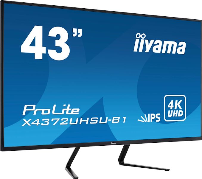
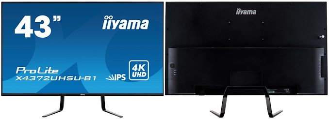
| 8:00a | Going Big: Iiyama Intros 43-inch ProLite X4372UHSU-B1 4K Monitor
Using a TV-sized display as a monitor always seemed like a fanciful idea. Until one day it wasn't. Thanks to the increasing commoditization of LCD panels and the continual downward pressure that has put on monitor prices, demand for large format monitors has been growing just as fast as monitors themselves. And while these kinds of large monitors are still far from ubiquitous, they've become an increasingly common sight in the monitor market. Besides making them more accepted in general, one of the benefits of the normalization of large format monitors is that it's enticed more manufacturers to enter the field. And now, Iiyama, a respected display maker, has become the latest vendor to jump into the market, introducing their own 42.5-inch monitor for work and play. Iiyama’s ProLite X4372UHSU-B1 is a 42.5-inch monitor featuring an IPS panel with a 3840x2160 resolution. The display features a typical brightness of 450 nits, a 1300:1 contrast ratio, a 4 ms response time, and a 60 Hz refresh rate. The monitor can reproduce 1.07 million of colors and is listed as supporting HDR, but the manufacturer doesn't list how much of the DCI-P3 gamut the monitor can reproduce, only noting that the LCD can cover 85% of the NTSC color gamut.
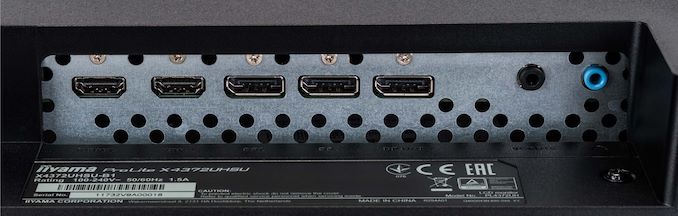
The manufacturer is positioning its ProLite X4372UHSU-B1 monitor for a wide range of applications, including CAD/CAM, entertainment, photography, and visualization. To that end, the monitor supports picture-by-picture and picture-in-picture capabilities, and comes with a total of four inputs: two DisplayPort 1.2 inputs, as well as two HDMI 2.0 ports. The monitor also has an outbound DisplayPort for daisy-chaining it with another LCD. In addition, the device has a quad-port USB hub supporting two 3.0 and two 2.0 connectors. On the audio side of matters, the LCD has two 9 W speakers, a line in as well as a headphone output.
Like many other large-sized monitors, the Iiyama ProLite X4372UHSU-B1 comes with a modest stand that can only adjust tilt. The good news, at least, is that it supports VESA mounts, so it can be used with a third party stands if necessary.
The ProLite X4372UHSU-B1 is currently available from European retailers for around €480.
Related Reading: | ||||||||||||||||||||||||||||||||||||||
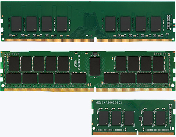
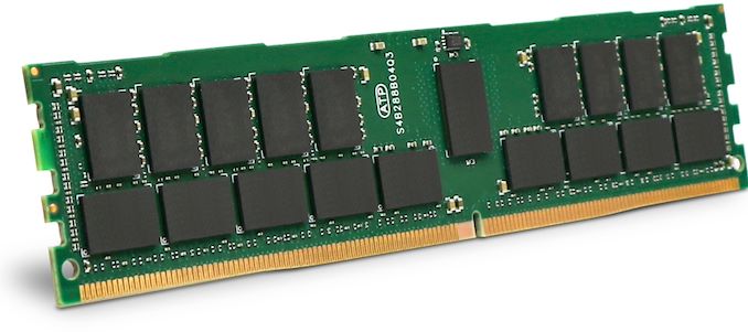
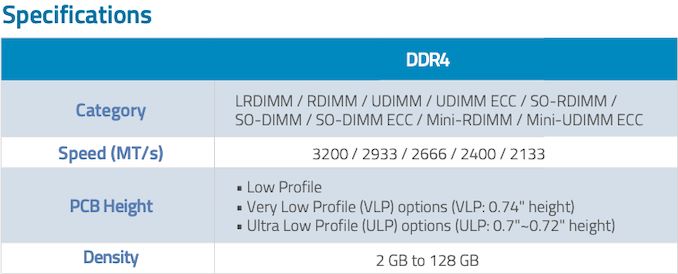
| 11:00a | ATP’s DDR4-3200 Industrial DIMMs: Up to 128GB @ 1.2V for AMD & Intel
ATP has unveiled its latest memory modules for servers and industrial applications, boasting a 3200 MT/s data transfer rate, an industry-standard voltage, and capacities ranging from 2 GB to 128 GB. The modules are available in various form-factors and configurations to address a variety of designs. ATP’s family of server/embedded/industrial DDR4-3200 at 1.2 V memory modules are validated to work with AMD’s EPYC 7002-series as well as Intel’s 2nd Generation Xeon Scalable CPUs, and are ready for AMD’s upcoming Milan and Genoa CPUs, as well as Intel’s Cooper Lake and Ice Lake processors. ATP uses a variety of certified memory chips for different modules featuring capacities ranging from 2 GB to 128 GB (e.g., the former uses 4 Gb chips, whereas the latter relies on 16 Gb dies).
The industrial-grade modules from ATP use special PCBs featuring thicker gold contacts, PCB underfill, conformal coating, and anti-sulfur resistors that are meant to protect DIMMs from shock/vibration, electromagnetic disturbance, humidity, and harsh chemicals in the air. Also, like other industrial components they are rated for extreme temperatures from –40°C to +85°C. Last but not least, these modules undergo module-level test during burn-in (TDBI) to reveal weak DIMMs that can produce errors.
Given that ATP’s family of DDR4-3200 at 1.2 V modules for server/embedded/industrial are aimed at a variety of designs, they come in LRDIMM, RDIMM, UDIMM, UDIMM ECC, SO-RDIMM, SO-DIMM, SO-DIMM ECC, Mini-RDIMM, and Mini-UDIMM ECC form-factors. Meanwhile, unbuffered DDR4-3200 modules are available in SO-DIMM, UDIMM, ECC UDIMM, ECC SO-DIMM, and RDIMM configurations. The new DDR4-3200 DIMMs from ATP are expected to be available shortly, at prices that will depend on configurations and form-factors. Related Reading: Source: ATP | ||||||||||||||||||||||||||||||||||||||
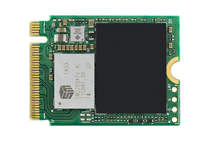
| 12:00p | SSSTC Launches CL1 M.2-2230 SSD: SMI, Up to 512 GB, Up to 2 GB/s
As notebooks are getting thinner and smaller, PC manufacturers require smaller components and therefore demand tinier SSDs as well as densely-packed SoCs. BGA SSDs are of course among the most compact storage devices around, but modular drives offer flexibility for PC manufacturers as well as end-users. To address this need, in recent years SSD vendors have started to offer M.2-2230 form-factor drives for client computers. This week, Kioxia-owned SSSTC unveiled its new CL1 M.2-2230 SSD that is not only fast, but is interesting for other capabilities as well. The SSSTC CL1 M.2-2230 SSD is based on Silicon Motion’s SM2263XT controller (NVMe, quad-channel, DRAM-less, TCG, AES, PCIe 3.0 x4) and carries 128 GB, 256 GB, and 512 GB of usable 3D TLC NAND memory. The drive is rated for up to 2000 MB/s sequential read speed as well as up to 1100 MB/s sequential write speed, which is in line with what other ultra-compact SSDs offer. Solid State Storage Technology Corp. (SSSTC) is a former SSD division of Lite-On that was acquired by Kioxia Holdings (formerly Toshiba Memory) last September. Toshiba Memory itself often used rebadged or customized controllers from Phison for its SSDs, so usage of SMI’s SM2263XT is interesting. What is also noteworthy is that the Kioxia BG4 SSD (available in M.2-2230 and BGA M.2-1620 form-factors) is actually rated for higher sequential speeds. As a result, Kioxia now has two products competing for the same niche market segment. SSSTC’s CL1 drives will likely be available shortly, but prices are currently unknown. Related Reading: Source: SSSTC (via Hermitage Akihabara) | ||||||||||||||||||||||||||||||||||||||
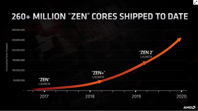
| 4:56p | AMD Shipped 260 Million Zen Cores by 2020
Today’s Financial Analyst Day 2020 from AMD is full of small nuggets of information. With the company building its foundation on its new x86 Zen high-performance architecture, keeping track of the finances is a good marker to find out how well its products are doing. Another marker is how many chips are in the wild. To that end, AMD's CTO Mark Papermaster presented this graph:
Since the launch of the first Zen products in 2017, the company states that it has shipped 260,000,000 Zen cores to date. It is worth noting that this is cores, not chips, and so there’s a mix of everything from 2-core to 64-core products in there. But this counts consumer, enterprise, commercial, and mobile products. With the launch of the Zen 2 based consoles later this year, this number is expected to shoot up by a significant margin. Side reading this graph, we get the following numbers: 2017-2018: ~30m cores Interested in more of our AMD Financial Analyst Day 2020 Coverage? Click here. | ||||||||||||||||||||||||||||||||||||||
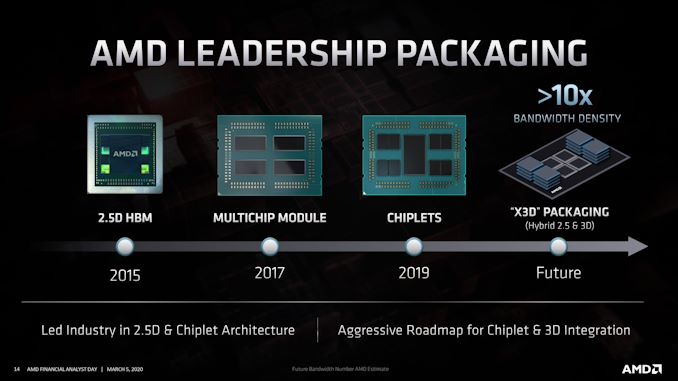
| 5:00p | AMD Discusses ‘X3D’ Die Stacking and Packaging for Future Products: Hybrid 2.5D and 3D
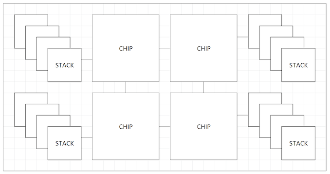
One of AMD’s key messages at its Financial Analyst Day 2020 is that the company wants to remain on the leading edge when it comes to process node technology as well as the latest packaging technology on its newest products. To that end, AMD discussed how it has surged forward with not only 2.5D interposer designs in its GPUs, but also stacked memory and chiplet implementations. The next stage of this journey, according to AMD, is a new X3D die stacking and packaging technology. The nature of the Financial Analyst Day means that AMD didn’t go into too much detail here, aside from a few diagrams, but the company was clear that it sees its aggressive roadmap for chiplet and 3D integration to lead to this X3D design, where the X stands for ‘hybrid’. AMD’s diagrams show four main compute chiplets, arranged in a 2x2 pattern, and then 4-high stacked die with one per chiplet. All of these chips are then on a large interposer underneath.
In this case, it seems that the ‘die stacking’ element points to HBM or some form of memory, while the compute chiplets in the middle are only one high, but all connected through the interposer. AMD is claiming that this level of integration offers a 10x increase in bandwidth density, allowing more data to be shuttled from the memory stacks into the cores (and hopefully from storage into the memory stacks too). The new packaging technology was listed as ‘future’, with no confirmed date. With AMD today announcing its new CDNA architecture for programmable compute graphics solutions, that sort of product would fit in really well here. With AMD’s prowess in CPU chiplet design, there could also be additional scope in future enterprise CPU developments as well. Graphics is a bit more farfetched, as the chiplet paradigm in graphics is a tricky one to solve. We asked AMD more information about it, as to whether it correlates to any of TSMC’s latest packaging developments such as CoWoS or LIPINCON, however AMD stated that more would be detailed closer to the time at a dedicated event. We requested an AMD Architecture Day as soon as travel will allow. More to come as we find out about it. Interested in more of our AMD Financial Analyst Day 2020 Coverage? Click here. | ||||||||||||||||||||||||||||||||||||||
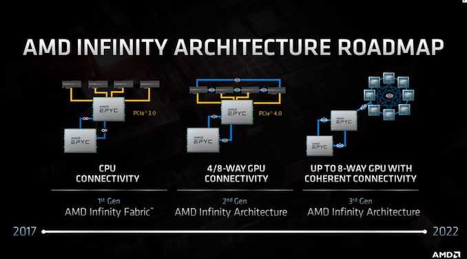
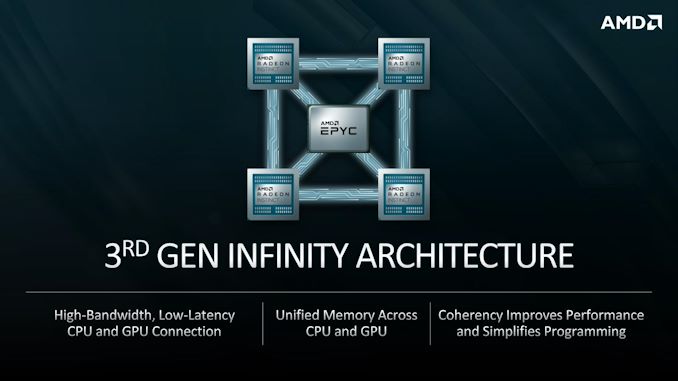
| 5:15p | AMD Moves From Infinity Fabric to Infinity Architecture: Connecting Everything to Everything
Another element to AMD’s Financial Analyst Day 2020 was the disclosure of how the company intends to evolve its interconnect strategy with its Infinity Fabric (IF). The plan over the next two generations of products is for the IF to turn into its own architectural design, no longer just between CPU-to-CPU or GPU-to-GPU, and future products will see a near all-to-all integration. AMD introduced its Infinity Fabric with the first generation of Zen products, which was loosely described as a superset of Hypertransport allowing for fast connectivity between different chiplets within AMD’s enterprise processors, as well as between sockets in a multi-socket server. With Rome and Zen 2, the company unveiled its second generation IF, providing some more speed but also GPU-to-GPU connectivity.
This second generation design allowed two CPUs to be connected, as well as four GPUs to be connected in a ring, however the CPU-to-GPU connection was still based in PCIe. With the next generation, now dubbed Infinity Architecture, the company is scaling it not only to allow for an almost all-to-all connection (6 links per GPU) for up to eight GPUs, but also for CPU-to-GPU connectivity. This should allow for a magnitude of improved operation between the two, such as unified memory spaces and the benefits to come with that. AMD is citing a considerable performance uplift with this paradigm.
AMD and LLNL recently disclosed that the new El Capitan supercomputer will have the latest generation Infinity Architecture installed, with 1 Zen 4-based Genoa EPYC CPU to 4 GPUs. This puts the timeline for this feature in the ballpark of early 2022.
Interested in more of our AMD Financial Analyst Day 2020 Coverage? Click here. | ||||||||||||||||||||||||||||||||||||||
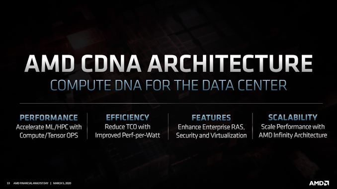
| 5:25p | AMD Unveils CDNA GPU Architecture: A Dedicated GPU Architecture for Data Centers
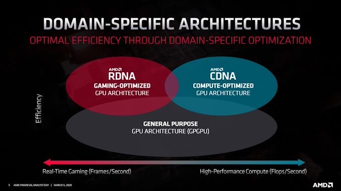
Over the last decade, the industry has seen a boom in demand for GPUs for the data center. Driven in large part by rapid progress in neural networking, deep learning, and all things AI, GPUs have become a critical part of some data center workloads, and their role continues to grow with every year. Unfortunately for AMD, they’ve largely been bypassed in that boom. The big winner by far as been NVIDIA, who has gone on to make billions of dollars in the field. Which is not to say that AMD hasn’t had some wins with their previous and current generation products, including the Radeon Instinct series, but their share of that market and its revenue has been a fraction of what NVIDIA has enjoyed. AMD’s fortunes are set to change very soon, however. We already know that AMD (as a supplier to Cray) has scored two big supercomputer wins with the United States – totaling over $1 billion for CPUs and GPUs – so there have been a lot of questions on just what AMD has been working on that has turned the heads of the US government. The answer, as AMD is revealing today, is their new dedicated GPU architecture for data center compute: CDNA. The Compute counterpart to the gaming-focused RDNA, CDNA is AMD’s compute-focused architecture for data center and other uses. Like everything else being presented at today’s Financial Analyst Day, AMD’s reveal here is at a very high level. But even at that high level, AMD is making it clear that there’s a fission of sorts going on in their GPU development process, leading to CDNA and RDNA becoming their own architectures.
Just how different these architectures are (and over time, will be) remains to be seen. AMD has briefly mentioned that CDNA is going to have less “graphics-bits”, so it’s likely that these parts will have limited (if any) graphics capabilities, making them quite dissimilar from RDNA GPUs in some ways. So broadly speaking, AMD is now on a path similar to what we’ve seen from other GPU vendors, where compute GPUs are increasingly becoming a distinct class of product, as opposed to repurposed gaming GPUs. AMD’s goals for CDNA are simple and straightforward: build family of big, powerful GPUs that are specifically optimized for compute and data center usage in general. This is a path AMD already started to go down with GPUs such as Vega 20 (used in the Radeon Instinct MI 50/60), but now with even more specialization and optimization. A big part of this will of course be machine learning performance, which means supporting faster execution of smaller data types (e.g. INT4/INT8/FP16), and AMD even goes as far as to explicitly mention tensor ops. But this can’t come at the cost of traditional FP32/FP64 compute either; those supercomputers that AMD’s GPUs will be going in will be doing a whole lot of high precision math. So AMD needs to perform well across the compute and machine learning spectrum, across many data types. To get there, AMD will also need to improve their performance-per-watt, as this is an area they have frequently trailed at. Today’s Financial Analyst Day announcement isn’t going into any real detail on how AMD is going to do this – beyond the obvious improvements in manufacturing processes, at least – but AMD is keenly aware of their need to improve. All the while CDNA will also differentiate itself with features, including some things only AMD can do. Enterprise-grade reliability and security will be one leg here, including support for ever-popular virtualization needs.
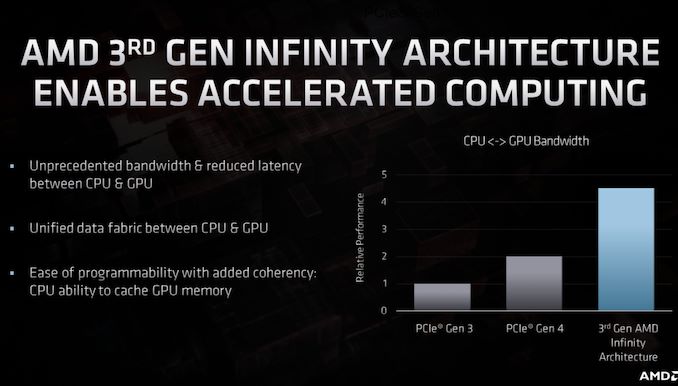
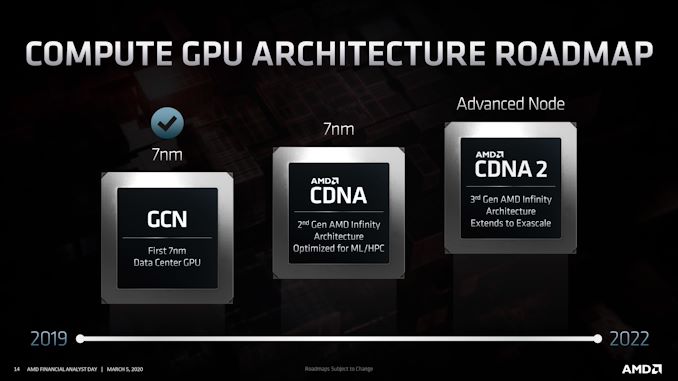
But AMD will also be leaning on their Infinity Fabric to give them an edge in performance scaling and CPU/GPU integration. Infinity Fabric has been a big part of AMD’s success story this far on the CPU side of matters, and AMD is applying this same logic to the GPU side of matters. This means using IF to not only link GPUs to other GPUs, but using IF to link GPUs to CPUs. Which is something we’ve already seen in the works for AMD’s supercomputer wins, where both systems will be using IF to team up 4 GPUs with a single CPU. AMD’s big win, however, will be a bit further down the line, when their 3rd gen Infinity Fabric is ready. It’s at that point where AMD intends to deliver a fully unified CPU/GPU memory space, fully leveraging their ability to provide both the CPUs and GPUs for a system. Unified memory can take a few different forms, so there are some important details that are missing here that will be saved for another day, but ultimately having a unified memory space should make programming heterogenous systems a whole lot easier, which in turn makes incorporating GPUs into servers all the better choice. And since CNDA is now its own branch of AMD’s GPU architecture – with command of it falling under data center boss Forrest Norrod, interestingly enough – it also has its own roadmap with multiple generations of GPUs. With AMD treating Vega 20 as the branching point here, the company is revealing two generations of CDNA to come, aptly named CDNA (1) and CDNA 2.
CDNA (1) is AMD’s impending data center GPU. We believe this to be AMD’s “Arcturus”, and according to AMD it will be optimized for machine learning and HPC uses. This will be an Infinity Fabric-enabled part, using AMD’s second-generation IF technology. Keeping in mind that this is a high level overview, at this point it’s not super clear whether this part is going in either of AMD’s supercomputer wins; but given what we know so far about the later El Capitan – which is now definitely using CDNA 2 – CNDA (1) may be what’s ending up in Frontier. Following CDNA (1) of course is CDNA 2. AMD is not sharing too much in the way of details here – after all, they haven’t yet shipped the first CDNA let alone the second – but they have confirmed that it will incorporate AMD’s third generation Infinity Fabric. As well, it will use a newer manufacturing node, which AMD is calling "Advanced Node" for now, as they are not disclosing the specific node they intend to use. So in a few different respects, CDNA 2 will be the piece de resistance of AMD’s heterogeneous compute plans, where they finally get to have a unified, coherent memory system across discrete CPUs and GPUs. As for shipping dates, while AMD isn’t disclosing exact dates at this time, the roadmap itself only extends to the end of 2022, meaning that AMD expects to be shipping CDNA 2 in volume by then. This aligns fairly well with this week’s El Capitan announcement, which has the supercomputer being delivered in 2023. Overall, AMD has some significant ambitions for their future data center GPUs. And while they have a lot of catching do to realize those ambitions, they’ve certainly laid out a promising roadmap to get there. AMD isn’t wrong about the importance of the data center market from both a technology perspective and a revenue perspective, and having a dedicated branch of their GPU architecture to get there may be just what AMD needs to finally find the success they seek. | ||||||||||||||||||||||||||||||||||||||
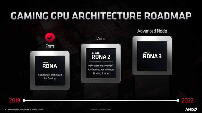
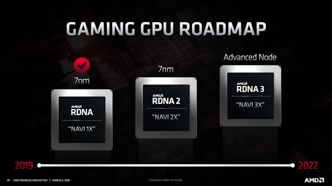
| 5:35p | AMD's 2020-2022 Client GPU Roadmap: RDNA 3 & Navi 3X On the Horizon With More Perf & Efficiency
As has become something of a tradition for AMD, this year’s Financial Analyst Day included a high level update to the company’s GPU roadmap. The last roadmap we saw from AMD, unveiled back at the Radeon RX 5700 XT launch last summer, went as far as RDNA 2. Now with RDNA 2 (Navi 2X) set to launch this year, AMD has extended the roadmap to include what’s next. And what’s next is RDNA 3. The successor to RDNA 2, RDNA 3 will build off of what AMD will achieve in the coming quarters with their forthcoming GPU architecture. With RDNA 2 not off the ground yet, for obvious reasons AMD is saying very little about RDNA 3 at this time, especially with regards to features. But what we do know is that, like RDNA 2, AMD is targeting continual perf-per-watt increases, as power consumption remains the ultimate bottleneck to total GPU performance. Helping AMD get there will be a new process node. For now the company is not disclosing which node it will be, using “Advanced Node” as a catch-all for what they decide to use. Coming off of TSMC’s 7nm process they will have several options to use, including TSMC’s 6nm and 5nm processes. And given TSMC’s roadmaps, it’s more or less inevitable that this will be the point where AMD begins using an EUV-based process for their GPUs, as AMD has indicated that this year’s RDNA 2 will not be using TSMC’s EUV-based 7nm+ process. Overall AMD has a lot of work ahead of them. While RDNA (1) and Navi 1X helped to reinvigorate AMD last year, the company is still struggling to reestablish itself as a fully viable top-to-bottom competitor to market leader NVIDIA. AMD currently trails on hardware features, while their overall perf-per-watt is currently competitive, but due in part to AMD having an atypical advantage in manufacturing nodes. So continuing to quickly iterate their GPU architecture to improve both features and their overall perf-per-watt – including moving to newer manufacturing nodes – is exactly what the company needs to do in order to become the market leader they desire to be. On the whole it’s very Zen-like, and this is clearly intentional. Meanwhile it’s interesting to see that AMD is going to keep the Navi architecture name leading into RDNA 3. With the architecture set to include numerous new features compared to RDNA (1) as well as a new process node, we’d normally see a naming break at some point along that line. As more details come out about AMD’s next two GPU architectures, we’ll find out more about just what AMD is changing and improving. | ||||||||||||||||||||||||||||||||||||||
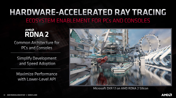
| 5:45p | AMD's RDNA 2 Gets A Codename: “Navi 2X” Comes This Year With 50% Improved Perf-Per-Watt While AMD’s Financial Analyst Day is first and foremost focused on the company’s financial performance – it’s right there in the title – this doesn’t stop the company from dropping a nugget or two of technical information along the way, to help excite investors on the future of the company. One such nugget this year involves AMD’s forthcoming RDNA 2 family of client GPUs. The successor to the current RDNA (1) “Navi” family, RDNA 2 has been on AMD’s roadmap since last year. And it’s been previously revealed that, among other things, it will be the GPU architecture used in Microsoft’s forthcoming Xbox Series X gaming console. And while we’re still some time off from a full architecture reveal from AMD, the company is offering just a few more details on the architecture. First and foremost, RDNA 2 is when AMD will fill out the rest of its consumer product stack, with their eye firmly on (finally) addressing the high-end, extreme performance segment of the market. The extreme high end of the market is small in volume, but it’s impossible to overstate how important it is to be seen there – to be seen as competing with the best of the best from other GPU vendors. While AMD isn’t talking about specific SKUs or performance metrics at this time, RDNA 2 will include GPUs that address this portion of the market, with AMD aiming for the performance necessary to deliver “uncompromising” 4K gaming.
But don’t call it "Big Navi". RDNA 2 isn’t just a series of bigger-than-RDNA (1) chips. The GPUs, which will be the codename “Navi 2X” family, also incorporate new graphics features that set them apart from earlier products. AMD isn’t being exhaustive here – and indeed they’re largely already confirming what we know from the Xbox Series X announcement – but hardware ray tracing as well as variable rate shading are on tap for RDNA 2. This stands to be important for AMD at multiple levels, not the least of which is closing the current feature gap with arch-rival NVIDIA.
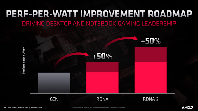
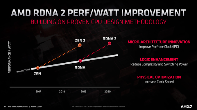
And AMD didn’t stop there, either. Even to my own surprise, AMD isn’t just doing RDNA (1) with more features; RDNA 2 will also deliver on perf-per-watt improvements. All told, AMD is aiming for a 50% increase in perf-per-watt over RDNA (1), which is on par with the improvements that RDNA (1) delivered last year. Again speaking at a high level, these efficiency improvements will come from several areas, including microarchitectural enhancements (AMD even lists improved IPC here), as well as optimizations to physical routing and unspecified logic enhancements to “reduce complexity and switching power.”
Process nodes will also play some kind of a role here. While AMD is still going to be on a 7nm process here – and they are distancing themselves from saying that they'll be using TSMC’s EUV-based “N7+” node – the company has clarified that they will be using an enhanced version of 7nm. To what extent those enhancements are we aren’t sure (possibly using TSMC’s N7P?), but AMD won’t be standing still on process tech. This strong focus on perf-per-watt, in turn, will be a key component of how AMD can launch itself back into being a fully viable, top-to-bottom competitor with NVIDIA. While AMD is already generally at parity with NVIDIA here, part of that advantage comes from an atypical advantage in manufacturing nodes that AMD can’t rely on keeping. NVIDIA isn’t standing still for 2020, and neither can AMD. Improving power efficiency for RDNA 2 (and beyond) will be essential for convincingly beating NVIDIA.
Overall, AMD has significant ambitions with RDNA 2, and it shows. The architecture will be the cornerstone of a generation of consoles, and it will be AMD’s first real shot in the last few years at taking back the flagship video card performance crown. So we’re eagerly awaiting to see what else RDNA 2 will bring to the table, and when this year the first video cards based on the new architecture will begin shipping. | ||||||||||||||||||||||||||||||||||||||
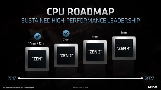
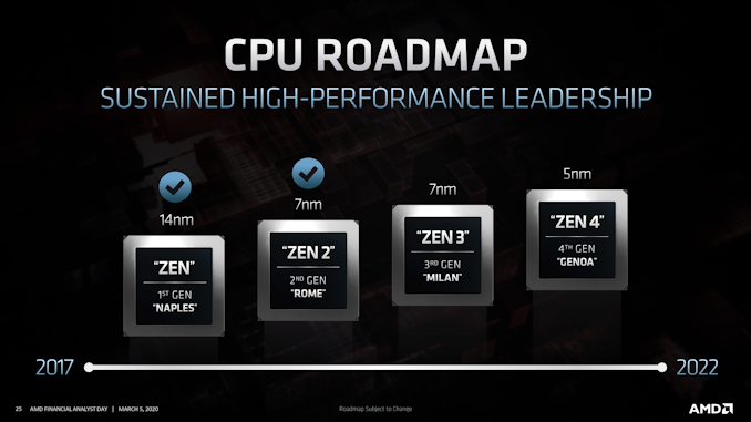
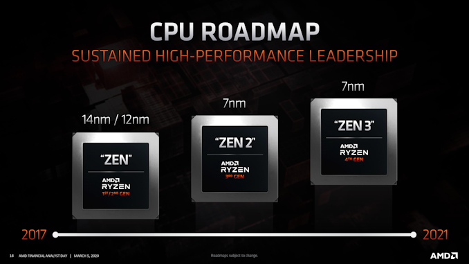
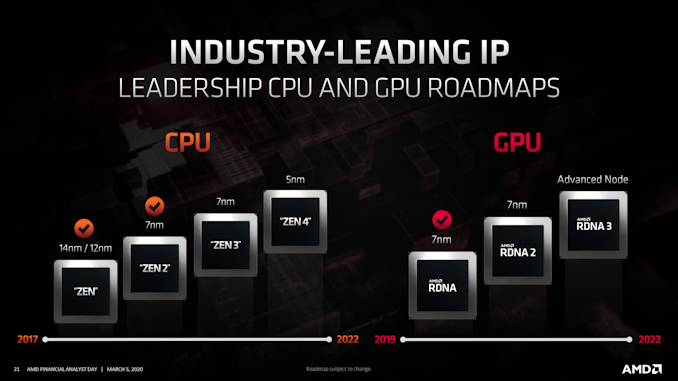
| 6:40p | Updated AMD Ryzen and EPYC CPU Roadmaps March 2020: Milan, Genoa, and Vermeer
Everyone is interested in roadmaps – they give us a sense of an idea of what is coming in the future, and for the investors, it gives a level of expectation as to where the company might be in a year to five years. Today at AMD’s Financial Analyst Day, the company gave the latest updates on the CPU side of the business, for consumer and for enterprise. AMD stated that its CPU roadmaps for its enterprise portfolio are going to offer more vision into the future than its consumer side for a couple of reasons. First, the enterprise market is built on a longer product cycle and it helps when planning these systems to know what is in the pipe publicly, but also from an investor standpoint where the enterprise market ultimately offers the bigger financial opportunity. To that end, AMD confirmed what we essentially knew, with Zen 3 based Milan coming in ‘late 2020’. Zen 4 based Genoa has already been announced as the CPU to power the El Capitan supercomputer, and in this roadmap AMD has put it as coming out by 2022. We asked AMD for clarification, and they stated that in this sort of graph, we should interpret it as the full stack of Genoa should be formally launched by the end of 2022. Given AMD’s recent 12-15 month cadence with the generations of EPYC, and the expected launch of Milan late this year, we would expect to see Genoa in early 2022.
Astute users might notice that Milan / Zen 3 has been listed as ‘7nm’, where previously it was listed as ‘7nm+’. We’ve got a whole news post on why AMD has made this change, but the short of it is that AMD initially put ‘7nm+’ to mean ‘an advanced version of 7nm’. When TSMC named its EUV version of 7nm as N7+, people had assumed they were the same, and AMD wanted to clarify that Milan is on a version of 7nm, and the exact version will be disclosed at a later date. In the future the company will avoid using ‘+’ so this doesn’t happen again (!). We also have Genoa listed as a 5nm product. Harder numbers about Milan and Genoa are expected to be unveiled closer to their respective launch times. On the consumer side, AMD said a little less, with its roadmap only going out to Zen 3, which has the codename ‘Vermeer’ for the desktop product.
In this graph, we see that the Zen 3 product here is on the far right, but so is the date – 2021. Does this mean Zen 3 for consumers is coming 2021? We asked AMD to clarify, and were told that we should interpret this as that the range of Zen 3 consumer products, such as desktop CPUs, HEDT CPUs, mobile APUs, and consumer APUs, should all be available by the end of 2021. The company clarified that Zen 3 will hit the consumer market ‘later this year’, meaning late 2020. So here comes a poignant question – what is going to come first in 2020? Zen 3 for enterprise is listed as ‘late 2020’, and Zen 3 for consumer is ‘later this year’. AMD makes a lot more money on its enterprise products than its consumer products, and while it enjoys a healthy performance lead in both, it really wants to push its market share in enterprise a lot more to drive home the bigger financial potential. With this in mind, I highly suspect that given AMD’s lead in the consumer market, we might see the company push more of its Zen 3 silicon into the enterprise market as a priority, with only a limited 2020 consumer release. I could be wrong, but we will find out closer to the time. Interested in more of our AMD Financial Analyst Day 2020 Coverage? Click here. | ||||||||||||||||||||||||||||||||||||||
| 6:50p | AMD Clarifies Comments on 7nm / 7nm+ for Future Products: EUV Not Specified
As part of AMD’s Financial Analyst Day 2020, the company gave the latest updates for its CPU and GPU roadmap. A lot of this we have seen before, with the company talking out to Zen 4 and Genoa on its datacenter CPU product line, out to Zen 3 and Ryzen 4000 with the consumer product line, and now with the RDNA/CDNA split between consumer and compute graphics. In previous graphs of a similar nature, AMD used the term ‘7nm+’ when referring to products beyond the first iteration of 7nm. AMD has today clarified to us that this does not mean they are using TSMC’s N7+ process node for those items. TSMC has three high-level versions of its 7nm process: This nomenclature has been finalized within the past year or so. Before this, AMD had presented various CPU and GPU roadmaps to the public. For the Zen 2 hardware, such as Ryzen 3000 series (Matisse), AMD had labeled this as ‘7nm’, which was all widely interpreted to mean TSMC’s N7 process. For future products, such as Zen 3, AMD had the slide listed as ‘7nm+’, which everyone had understood was ‘a better version of 7nm’.
Because AMD labeled those as 7nm+, when TSMC called its version of 7nm with EUV to be N7+, one of the obvious assumptions that people have made is that where AMD wrote 7nm+, it was to be on the N7+ process. We have since learned that this is not entirely correct. In order to avoid confusion, AMD is dropping the ‘+’ from its roadmaps. In speaking with AMD, the company confirmed that its next generations of 7nm products are likely to use process enhancements and the best high-performance libraries for the target market, however it is not explicity stating whether this would be N7P or N7+, just that it will be ‘better’ than the base N7 used in its first 7nm line.
This doesn’t necessarily mean that AMD isn’t going to be using EUV in the future – we were told it will be on a case by case basis, and at this time they wanted to clarify that AMD is not making any specific clarifications of which version of 7nm from TSMC it plans to use. More will be detailed at future events. Interested in more of our AMD Financial Analyst Day 2020 Coverage? Click here. | ||||||||||||||||||||||||||||||||||||||
| 8:15p | AMD Financial Analyst Day 2020 Round-Up: Laying A Path For Bigger & Better Things AMD’s first Financial Analyst Day since 2017 has just wrapped up. In the last three years AMD has undergone a dramatic change, launching its Zen CPU architecture, and greatly improving the trajectory of a company that was flirting with bankruptcy a few years ago. And now that AMD’s foundation is once again secure, the company has gathered to once again talk to its loyal (and looking at stock prices, now much richer) investors and how it’s planning to use this success to push into bigger and better things. We’ve been covering FAD 2020 throughout the afternoon, and we have seen AMD make a number of announcements and roadmap reveals throughout the event. The individual announcements are below, and meanwhile now that the event has wrapped up we want to provide a quick summary of what AMD is going to be up to over the next five years. | ||||||||||||||||||||||||||||||||||||||


| << Previous Day |
2020/03/05 [Calendar] |
Next Day >> |