[Most Recent Entries] [Calendar View]
Tuesday, October 22nd, 2019
- Synopsys to Accelerate Samsung’s 7nm Ramp with Yield Explorer Platform
- Samsung Foundry Updates: 8LPU Added, EUVL on Track for HVM in 2019
- New Tools & IP Accelerate Development of 5nm Arm ‘Hercules’ SoCs
- Samsung Starts Mass Production of Chips Using Its 7nm EUV Process Tech
- 32 GB Unbuffered DIMMs Listed from Seven Brands: DDR4-2400 to DDR4-3000
- G.Skill Launches 32 GB DDR4 Modules, 256 GB Kits: Up to DDR4-4000
- Corsair Unveils 32 GB Vengeance LPX DDR4 DIMMs, 64 GB & 128 GB Dual-Channel Kits
- Samsung 32GB DDR4-2666 Non-ECC Memory at Retail: $168
- ADATA Demonstrates 32 GB DDR4 Modules, Built on Micron 16 Gb
- Crucial 32 GB DDR4 Modules Found in an ASRock System
- GIGABYTE’s Aorus CV27Q Curved ‘Tactical’ Monitor: 165 Hz QHD With FreeSync 2
- AOC Agon 35-Inch 200 Hz Curved 3440x1440 HDR Gaming Monitor with FreeSync 2 or GSync
- AOC Announces AGON AG322QC4 32-Inch Curved LCD with FreeSync 2 & DisplayHDR 400
- HP's Omen X 27: A 240Hz QHD Monitor with FreeSync 2 HDR
- AOC’s Agon Monitors with 0.5ms Response Time & 240 Hz Refresh Now Available
- SK Hynix Reveals DDR4-3200 Memory Chips with 4 Phase Clocking
- SK Hynix to Start Using 2nd Gen 10nm-class DRAM Process Technology in 2H 2019
- SK Hynix Details DDR5-6400
- SK Hynix Develops First 16 Gb DDR5-5200 Memory Chip, Demos DDR5 RDIMM
| Time | Event | ||||||||||||||||||||||||||||||||||||||||||||
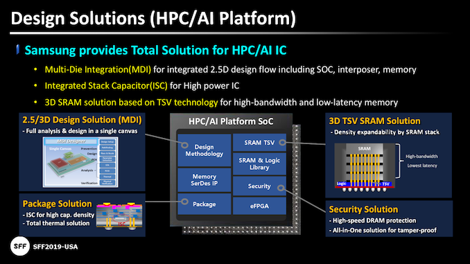
| 8:00a | New Tools Simplify Development of 2.5D Multi-Die 7nm Designs at Samsung Foundry
Advanced packaging technologies simplify production and increase performance of highly-complex multi-die SoCs as the semiconductor industry is looking at chiplet approach as an alternative to large dies that take a longer time long to develop and are expensive to make. But designing 2.5D multi-die chips has its own peculiarities, which is why Samsung Foundry and its rivals offer their clients a special 2.5D-IC Multi-Die Integration (MDI) design flow that incorporates analysis and implementation for early-stage system-level pathfinding to help overcome potential issues. This month support for Samsung 2.5D-IC MDI flow was added into Synopsys’ chip development software to simplify development process for engineers. Samsung Foundry currently offers 2.5D-IC MDI flow for chips produced using its 7LPP (7 nm with several EUV layers) fabrication process and its SUB20LPIN silicon interposer. According to the company, its 2.5D-IC MDI flow helps customers to solve issues like coupling noise between multi-die and package at early stages of design and therefore reduce turnaround time for solving issues (which in the end means lower development costs), overcoming performance problems, and speed up time-to-market. Samsung’s 2.5D-IC MDI flow is now supported by Synopsys’ Fusion Design Platform and Custom Design Platform software packages that are used to develop SoCs.
The programs feature automated silicon interposer creation and routing; routing among microbumps, TSVs, and C4 bumps; power network design; EM/IR analysis of multi-dies and interposer; automated SPICE deck generation for power; and signal integrity analysis of HBM and high-speed interfaces. Functionality of exact software suites is described in the table below.
By launching its 2.5D-IC MDI flow for 7LPP technology and SUB20LPIN silicon interposer, Samsung Foundry aims to simplify the development process for its customers who adopt multi-die/chiplet approach for their devices aimed at high-performance computing, AI, and other performance-demanding applications. Obviously, quite some time will pass before the first 2.5D devices designed using the 2.5D-IC MDI flow (and Synopsys software) will be brought to fruition, but this is a start. Here is what Michael Sanie, vice president of marketing and strategy for the Synopsys Design Group, had to say:
Related Reading: Source: Synopsys | ||||||||||||||||||||||||||||||||||||||||||||
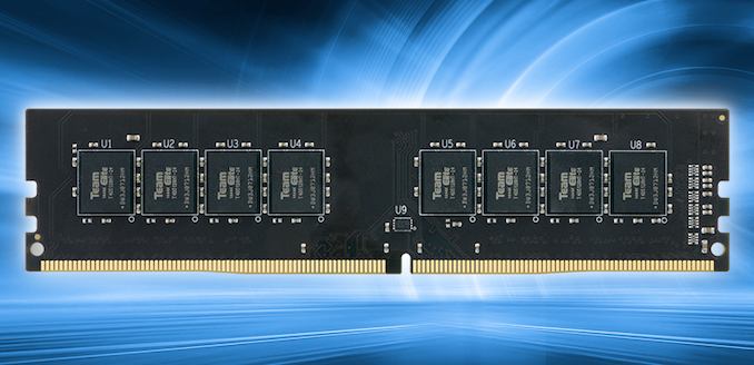
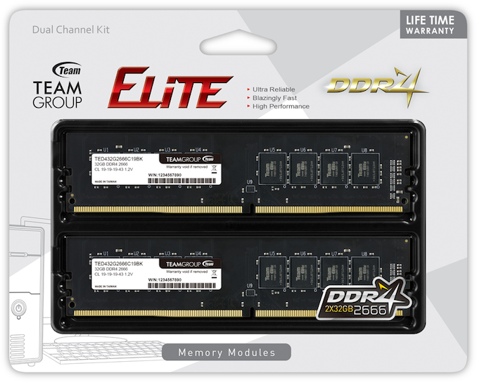
| 11:00a | Team Group Quietly Launches 32 GB DDR4 Memory Modules
Team Group has quietly added 32 GB unbuffered DDR4 memory modules to its product catalogue and plans to start sales in the near future. The modules will feature JEDEC-standard data transfer rates and will be aimed primarily at OEMs as well as high-end desktops and workstations that benefit from loads of RAM yet do not necessarily need extreme bandwidth. Team Group’s Team Elite UD-D4 32 GB DDR4 unbuffered DIMMs rely on 16 memory chips featuring a 16 Gb capacity from an unknown manufacturer. The memory modules are rated for DDR-2666 mode with CL19 19-19-43 timings at 1.2 V, which is fully compliant with JEDEC’s standards. The UDIMMs are not equipped with a heat spreader since they are not meant to be overclocked by the manufacturer.
Team Group will offer its Team Elite UD-D4 32 GB DDR4-2666 UDIMMs as single modules and as dual-channel kits. The former will be aimed primarily at computer makers that need to cut down their BOM cost, while the latter will sell to all kinds of clients that need a dual-channel 64 GB memory subsystem.
By offering 32 GB modules with standard JEDEC speed and timings, Team Group maximizes their compatibility with systems. Meanwhile, an important thing to remember about 32 GB UDIMMs is that they may require a BIOS update as not all motherboards support them out-of-box. Team Group’s 32 GB UDIMMs as well as dual-channel 64 GB (2×32 GB) kits will be available in Japan starting from October 25. Pricing is unknown, but expect it to be comparable to other DDR4-2666 32 GB modules/kits. Related ReadingSources: Aiuto-jp.co.jp (via momomo_us/Twitter), Team Group | ||||||||||||||||||||||||||||||||||||||||||||
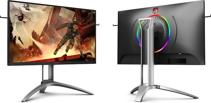
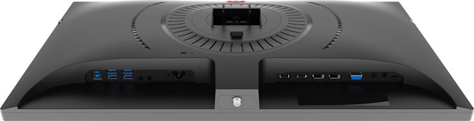
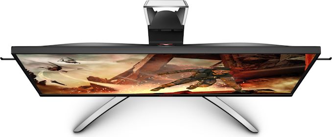
| 12:32p | AOC Reveals Agon AG273QX: A 27-Inch 165 Hz FreeSync 2 Monitor
AOC has introduced its new Agon-series 27-inch gaming display featuring a variable refresh rate of up to 165 Hz enabled by AMD’s FreeSync 2 technology. Like all Agon monitors, the AG273QX is aimed at demanding gamers and supports a multitude of features for the target audience, including special gaming modes, RGB lighting on the back, as well as G-Menu software for adjustments. The AOG Agon AG273QX display uses an 8-bit 27-inch VA panel featuring a 2560×1440 resolution, 400 nits peak brightness, a 3000:1 static contrast ratio, a maximum refresh rate of 165Hz, a 1 ms MPRT response time, and 178°/178° viewing angles. Being an AMD FreeSync 2-certified monitor, the AG273QX fully supports a variable refresh rate (presumably with a 48 Hz to 165 Hz), direct-to-display tonemapping, low framerate compensation (LFC) mode, and can hit 90% of the DCI-P3 color gamut. The LCD also meets DisplayHDR 400 requirements with an HDR brightness of 400 nits and supports at least HDR10 transport. Unfortunately, AOC does not disclose how many backlighting zones its new monitor has.
When it comes to connectivity, the Agon AG273QX has a D-Sub, two DisplayPort 1.2, one miniDisplayPort, and two HDMI 2.0 connector. In addition, it has a quad-port USB 3.0 hub, and a headphone output, which is common for gaming displays these days. As an added bonus, the monitor has two 5 W speakers.
Since the product is designed primarily for gamers, the Agon AG273QX not only features a stand that can adjust height, tilt, swivel, and even pivot, but also a handle for easy carrying. Meanwhile, it also supports three pre-configured game modes (FPS, RTS, Racing) as well as three customizable game modes. Last but not least, it also comes with G-Menu software to make adjustments without using the OSD buttons.
AOC will start sales of its Agon AG273QX in November. In the UK the product will cost £439, so expect its MSRP in the US to be around $499.
Related Reading: Source: AOC | ||||||||||||||||||||||||||||||||||||||||||||
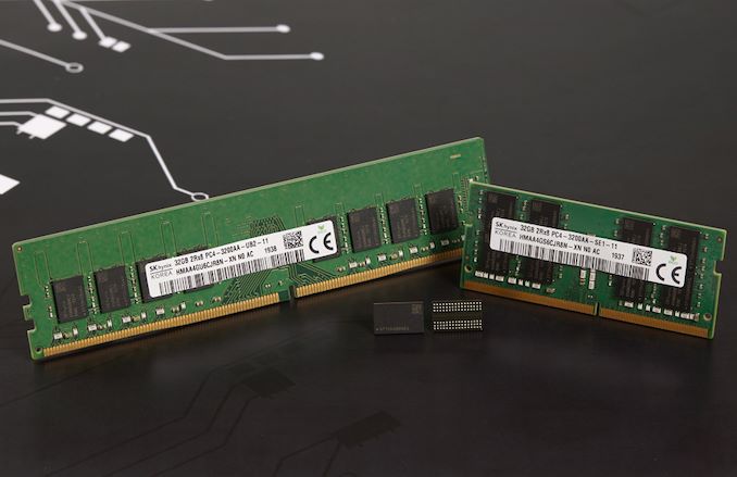
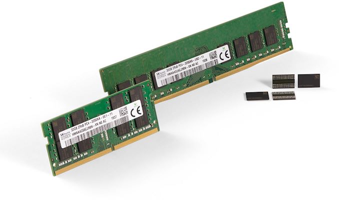
| 2:00p | SK Hynix Develops 16 Gb DDR4 Chips for 32 GB Modules
SK Hynix announced on Monday that it has completed development of its first monolithic 16 Gb chip. This chip is to be made using its 3rd Generation 10 nm-class process technology. The new memory devices will enable the company and its partners to make more energy-efficient and higher capacity DIMMs, such as 32 GB unbuffered modules for consumers or higher capacity buffered modules for enterprise consumption. SK Hynix’s 16 Gb chip made using the company’s 3rd Generation 10 nm-class manufacturing technology (also known as '1Z' nm) and is rated for DDR4-3200 data transfer rates. The company states that these chips have a reduced power consumption by 40% when compared to modules of the same capacity based on 8 Gb DRAMs produced using the company’s 2nd Generation 10 nm-class (aka 1Ynm) process. SK Hynix’s '1Z' nm process technology uses a new substance that enables it to maximize capacitance and improve stability of DRAM devices compared to previous generation process technology. It remains to be seen whether or not usage of the new chemicals translate into additional benefits, such as clock range, or latency. Also, the new technology enables a 27% higher bits-per-wafer productivity, which will make new memory chips cheaper to produce. The manufacturer stresses that its '1Z' nm process does not use extreme ultraviolet lithography (EUVL) and is still a fully DUV process.
In addition to its 16 Gb DDR4 chips, SK Hynix also introduced its 32 GB unbuffered DIMM and SO-DIMM modules that can be used by desktop computers. It is unclear when these modules are to be available, but it is logical to expect them to emerge after the 16 Gb DRAM devices hit mass production in 2020. The company plans to use its 1Znm process technology to make a variety DRAM types, including commodity DDR4 memory, LPDDR5, and HBM3. Related Reading: Source: SK Hynix | ||||||||||||||||||||||||||||||||||||||||||||


| << Previous Day |
2019/10/22 [Calendar] |
Next Day >> |