Войти в систему

Home
    - Создать дневник
    - Написать в дневник
       - Подробный режим

LJ.Rossia.org
    - Новости сайта
    - Общие настройки
    - Sitemap
    - Оплата
    - ljr-fif

Редактировать...
    - Настройки
    - Список друзей
    - Дневник
    - Картинки
    - Пароль
    - Вид дневника

Сообщества

Настроить S2

Помощь
    - Забыли пароль?
    - FAQ
    - Тех. поддержка


Пишет AnandTech ([info]syn_anandtech)
@ 2019-04-05 12:00:00


Previous Entry  Add to memories!  Tell a Friend!  Next Entry
TSMC’s 5nm EUV Making Progress: PDK, DRM, EDA Tools, 3rd Party IP Ready

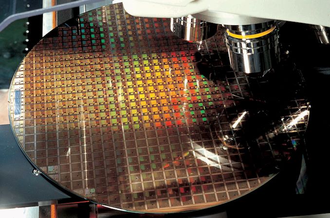
TSMC this week has said that it has completed development of tools required for design of SoCs that are made using its 5 nm (CLN5FF, N5) fabrication technology. The company indicated that some of its alpha customers (which use pre-production tools and custom designs) had already started risk production of their chips using its N5 manufacturing process, which essentially means that the technology is on-track for high-volume manufacturing (HVM) in 2020.


(Читать комментарии) (Добавить комментарий)