|
|
| Пишет AnandTech ( @ 2019-09-25 12:00:00 |
|
|
|
|
|
|
|
|
|
|
|
|
|
|
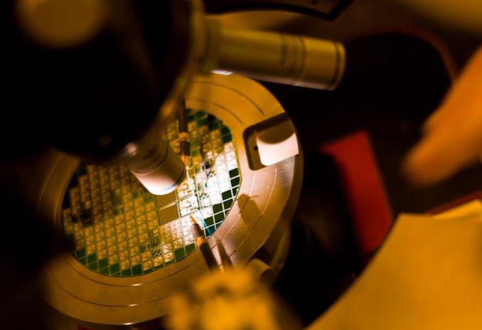
GlobalFoundries has introduced its 12LP+ fabrication process that relies on the groundwork set by its 14LPP and 12LP technologies and provides significant improvements when it comes to performance, power, and area (PPA) scaling. The specialty foundry positions the technology for developers of chips for cloud and edge AI applications.
GlobalFoundries’ 12LP+ manufacturing technology builds upon the company’s 12LP process yet enables a 20% increase in performance (at the same power and complexity) or a 40% reduction in power requirements (at the same clocks and complexity) as well as a 15% improvement in logic area scaling when compared to 12LP platform. Among other things, 12LP+ supports 0.5V SRAM bit cells (which probably use IP that the company designed for its 7 nm nodes). In addition, GF developed a new 2.5D interposer that enables 12LP+ SoCs to work with HBM memory.
| Advertised PPA Improvements of New Process Technologies Data announced by companies during conference calls, press briefings and in press releases |
||||||
| GlobalFoundries | ||||||
| 12LP+ vs 12LPP |
12LP vs 14LPP |
14HP vs 14LPP |
GF's 7nm Gen 1 vs 14LPP |
|||
| Power | 40% | - | ? | >60% | ||
| Performance | 20% | 10% | ? | >40% | ||
| Area Reduction | 15% | 15% | ? | >50% | ||
The foundry says that its 12LP+ uses a mature design and production ecosystem and provides advantages comparable to those of 7 nm-class fabrication process. Meanwhile, significant improvements and a new PDK point to new design libraries along with numerous new features, which means that GlobalFoundries’ clients will have to make significant investments in order to take advantage of 12LP+. Those investments will still be 50% lower than the cost of transition to a 7 nm-class technology, according to GlobalFoundries.
Michael Mendicino, vice president of Digital Technology Solutions at GF, said the following:
“Our 12LP+ solution already offers clients a majority of the performance and power advantages they would expect to gain from a 7nm process, but their NRE (non-recurring engineering) costs will average only about half as much, a significant savings. Additionally, because the 12 nm node has been running longer and is much more mature, clients will be able to tape-out quickly and take advantage of the growing demand for AI technology.”
To speed up development of 12LP+ chips for its clients, GlobalFoundries has asked Arm to design Arm Artisan physical IP and POP IP required by AI-focused SoCs. That IP is said to be compatible with 12LP. Meanwhile, the 12LP+ PDK is already available and several clients have begun to design chips using the technology. GlobalFoundries expects its customers to tape out the first 12LP+ SoCs sometimes in the second half of 2020 and produce them in volume in 2021.
GlobalFoundries will manufacture 12LP+ chips using deep ultraviolet (DUV) lithography with argon fluoride (ArF) excimer lasers operating on a 193 nm wavelength at its Fab 8 in New York, USA. Presumably, the company will use the same equipment that is currently used to make SoCs at 12LP and 14LPP nodes.
Related Reading:
- GlobalFoundries Adds 12LP Process for Mainstream and Automotive Chips; AMD Planning 12LP CPUs & GPUs
- GlobalFoundries Weds FinFET and SOI in 14HP Process Tech for IBM z14 CPUs
- GlobalFoundries Stops All 7nm Development: Opts To Focus on Specialized Processes
- Change of Strategy: A New GlobalFoundries CEO in Dr. Thomas Caulfield
- Samsung Details 11LPP Process Technology: 10 nm BEOL Meets 14 nm Elements
Source: GlobalFoundries