|
|
| Пишет AnandTech ( @ 2021-05-06 06:00:00 |
|
|
|
|
|
|
|
|
|
|
|
|
|
|
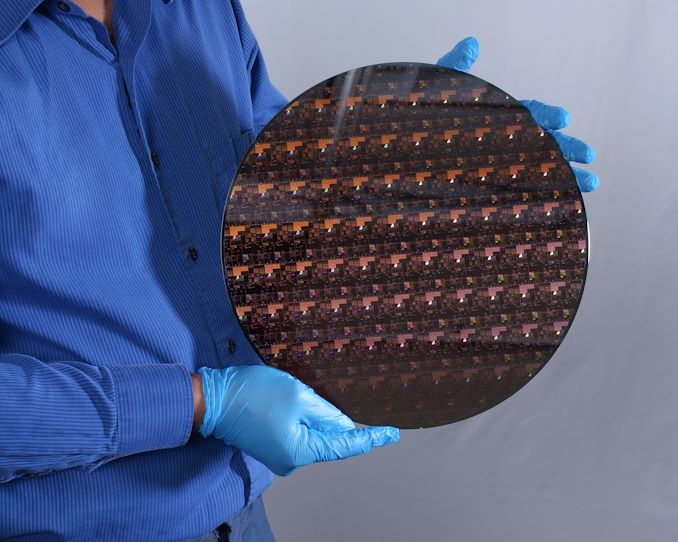
Every decade is the decade that tests the limits of Moore’s Law, and this decade is no different. With the arrival of Extreme Ultra Violet (EUV) technology, the intricacies of multipatterning techniques developed on previous technology nodes can now be applied with the finer resolution that EUV provides. That, along with other more technical improvements, can lead to a decrease in transistor size, enabling the future of semiconductors. To that end, Today IBM is announcing it has created the world’s first 2 nanometer node chip.