|
|
| Пишет AnandTech ( @ 2021-10-06 13:02:00 |
|
|
|
|
|
|
|
|
|
|
|
|
|
|
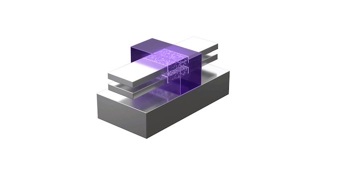
One of the key semiconductor technologies beyond 3D FinFET transistors are Gate-All-Around transistors, which show promise to help extend the ability to drive processors and components to higher performance and lower power. Samsung has always announced that its first generation GAA technology will align with its ‘3nm’ nodes, with its 3GAE and 3GAP processes. As part of the Samsung Foundry Forum today, some more insight was put into the timeline for the rollout, as well as talk of its 2nm process.