|
|
| Пишет AnandTech ( @ 2013-01-12 02:08:00 |
|
|
|
|
|
|
|
|
|
|
|
|
|
|
Earlier in the week Samsung announced the Galaxy S 2 Plus, a rather strange late-cycle update to the SGS2. The device is pretty much what you'd expect, and contains similar specs to the existing SGS2 — 1.2 GHz dual core SoC, 4.3-inch SAMOLED Plus WVGA display, Android 4.1.2, and quad band HSPA+ 21.1.
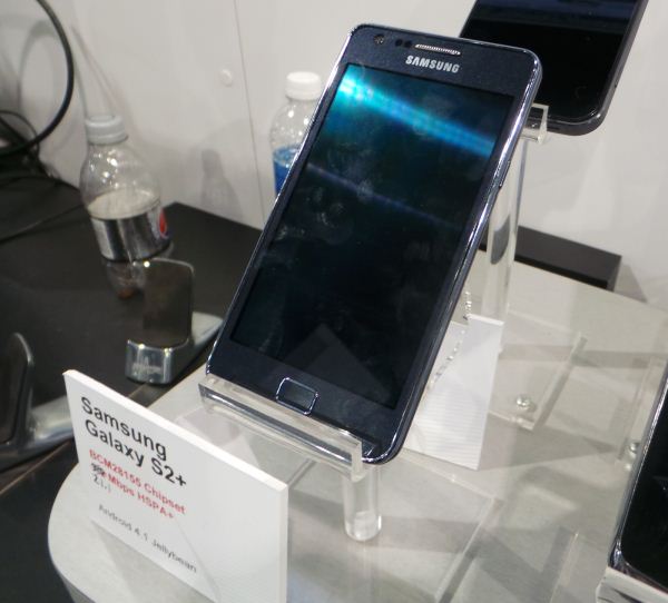
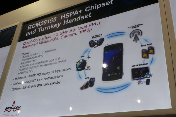
What was unknown about the Galaxy S 2 Plus was which SoC was inside. Originally I assumed this was just a respun Exynos 4 inside, but while I was at Broadcom's booth I noticed the Galaxy S 2 Plus on display, and noted that it includes a BCM28155 SoC inside.
BCM28155 consists of two 1.2 GHz ARM Cortex A9s alongside a two core Broadcom VideoCore IV solution. I'm unclear about fabrication process but suspect 40nm TSMC or so. The entire Galaxy S 2 Plus is one big Broadcom reference design as well, and I'm told this time Samsung finally ditched the discrete Fujitsu ISP in the place of Broadcom's on-SoC ISP. GLBenchmark 2.5.1 was already installed on the device, likely by a customer, however I had trouble getting the device to complete a run. The SGS2 Plus felt speedy, however, I wasn't able to do much in depth benchmarking.


Source: Samsung (Product Specs)
 |  |